Naphthalene tetracarboxylic diimide based polymer, electrophotographic photoreceptor containing the same, and electrophotographic cartridge, electrophotographic drum and electrophotographic image forming apparatus comprising the electrophotographic photoreceptor
a technology of tetracarboxylic diimide and polymer, which is applied in the direction of electrographic process, electrographic process apparatus, instruments, etc., can solve the problems of increasing exposure potential, voids, and entire photoconductive layer peeling, so as to inhibit the increase of exposure potential and minimize the effect of image defects
- Summary
- Abstract
- Description
- Claims
- Application Information
AI Technical Summary
Benefits of technology
Problems solved by technology
Method used
Image
Examples
preparation example
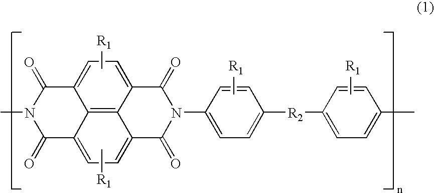
34 g (0.1 mol) of 4,4′-(hexafluoroisopropylidene)dianiline having formula (9) below and 26 g (0.1 mol) of 1,4,5,8-naphthalenetetracarboxylic anhydride were refluxed in 300 ml of DMF (dimethyl formamide) for 2 hours. After cooling the mixture to room temperature, 100 ml of a solution of 1:2 pyridine / acetic anhydride was added to the resulting solution and reacted at room temperature for 1 hour, then at 70° C. for 3 hours, followed by precipitating in 2000 ml of methanol. The precipitate was filtered and repeatedly purified by reprecipitating in methanol to obtain 35 g of the compound (I) having formula (6) (yield: about 60%).
example 1
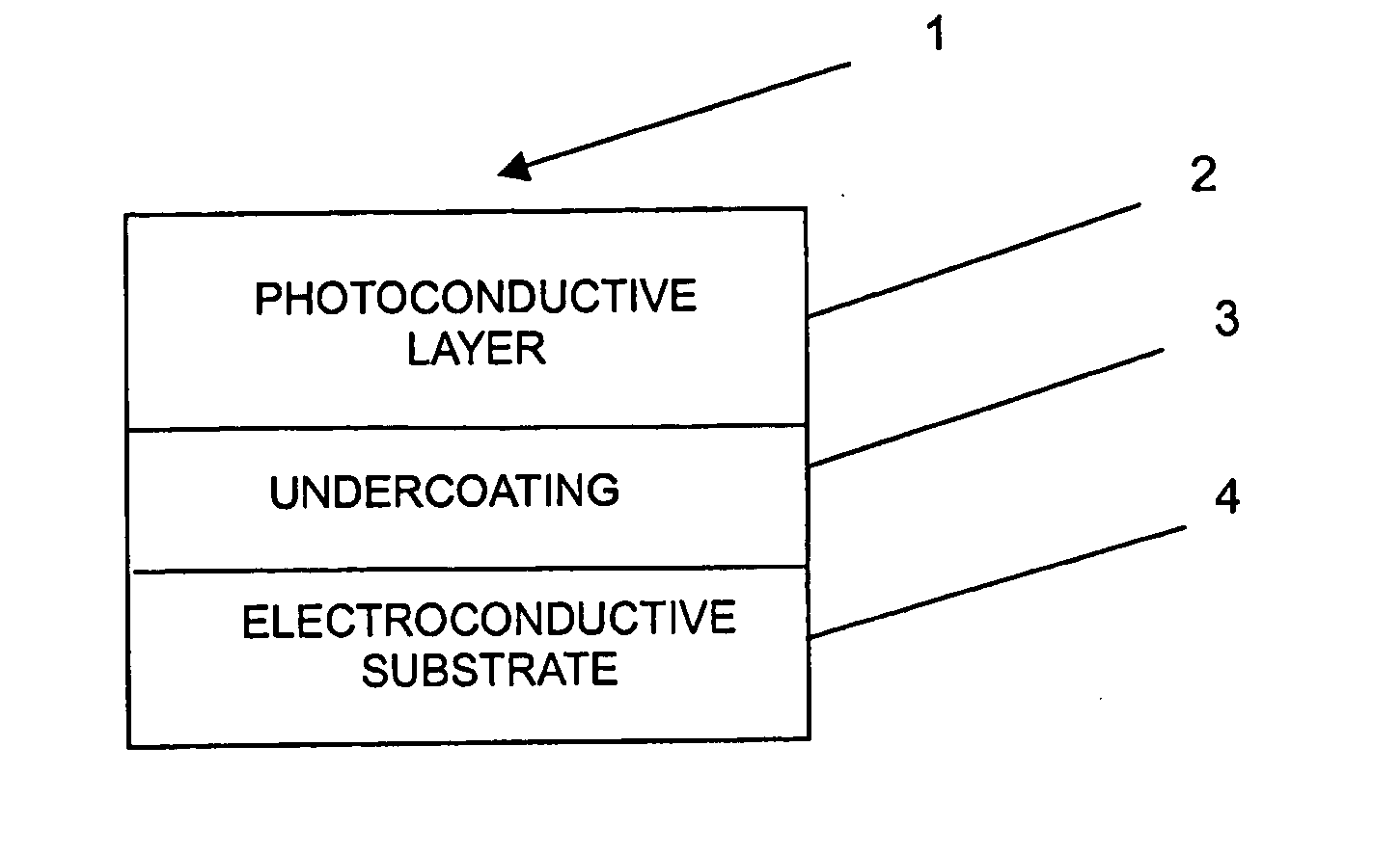
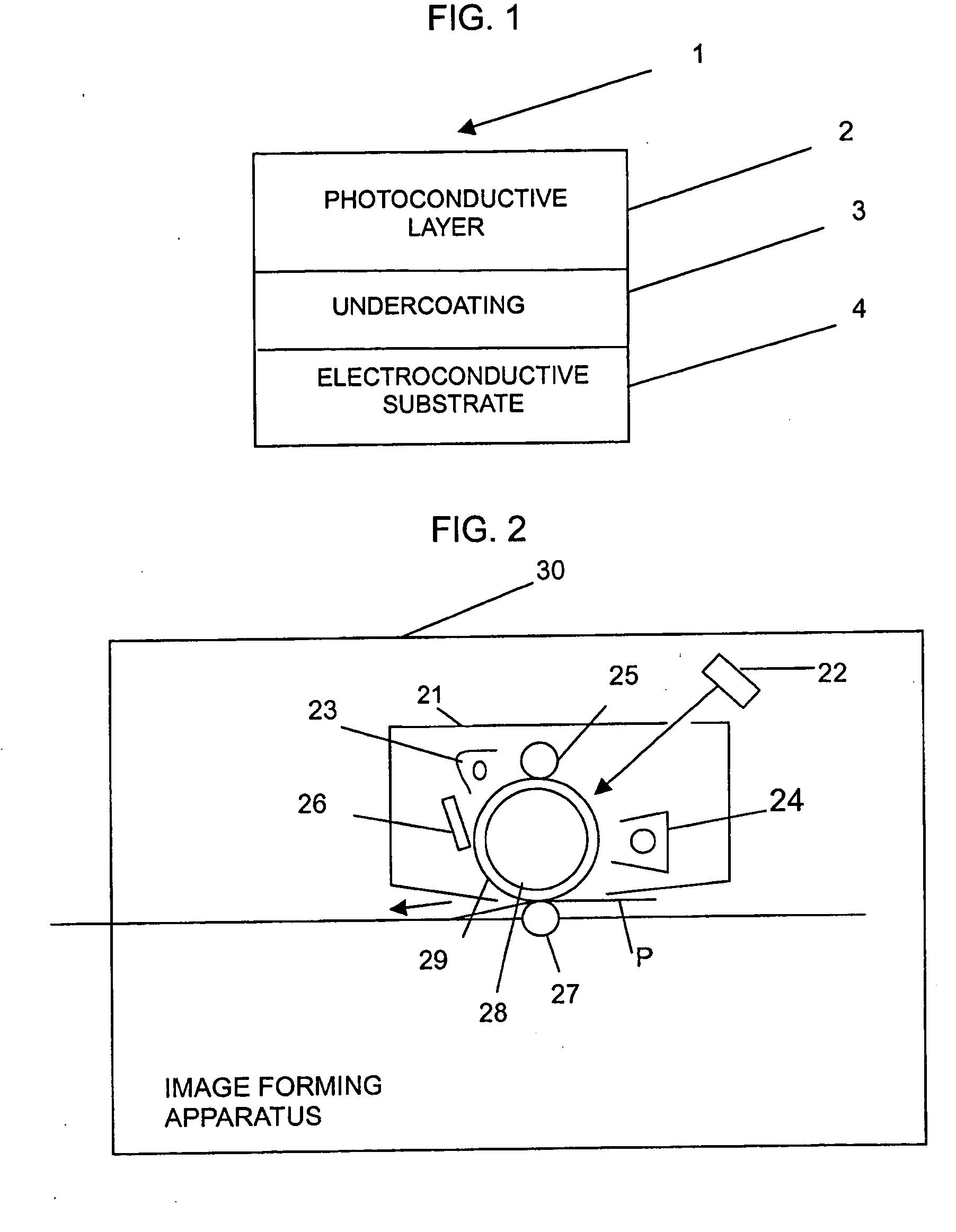
0.5 g of the compound (I) prepared in the above Preparation Example was dissolved in a solvent (9.5 g of THF, i.e., tetrahydrofuran)) and filtered (pore size=5 μm), and the solution was coated on an aluminum drum by a ring coating apparatus at a rate of 300 mm / min and dried at 70° C. for 30 minutes to form an undercoat having a thickness of about 2 μm.
3 g of milled gamma titanyl phthalocyanine (γ-TiOPc produced by H. W. SANDS, 15.23% by weight of ethanol) and 2 g of polyvinylbutyral resin (BX-1 produced by SEKISUKI) were added to 8.34 g of methylethylketone and filtered (pore size=5 μm), and the solution was coated on the undercoat by the ring coating apparatus at a rate of 300 mm / min and dried at 70° C. for 60 minutes to form a photoconductive layer having a thickness of about 1 μm. Thus, the charge generating layer was formed.
50 parts by weight of a hole transport material (MPCT 10 produced by MITSUBISHI PAPER MILLS) and 50 parts by weight of a binder resin (PCZ200 produced b...
experimental example
The charge potential and the exposure potential of each of the photoreceptors prepared in Example 1 and Comparative Examples 1 and 2 were measured using PDT-2000 manufactured by QEA. Each photoreceptor was charged by applying a voltage of 8 kV, and then exposed to an energy of 1 μJ / cm2. The charge potential (V) and the exposure potential (Vr) were measured at initial stage and after 500 cycles. The measurement results are shown in Table 1 below.
TABLE 1V0V0rV500V500rExample 1698.444.4721.389.4Comparative619.135.6586.851.1Example 1Comparative678.255.8676.9104.2Example 2
In the above Table 1, V0 and V500 represent the initial charge potential and the charge potential after 500 cycles, respectively, and V0r and V500r represent the initial exposure potential and the exposure potential after 500 cycles, respectively.
As shown in Table 1, the exposure potential of the photoreceptor of Example 1 according to an embodiment of the present invention increased less than that of the photorec...
PUM
| Property | Measurement | Unit |
|---|---|---|
| charge | aaaaa | aaaaa |
| charge transport | aaaaa | aaaaa |
| electroconductive | aaaaa | aaaaa |
Abstract
Description
Claims
Application Information


