

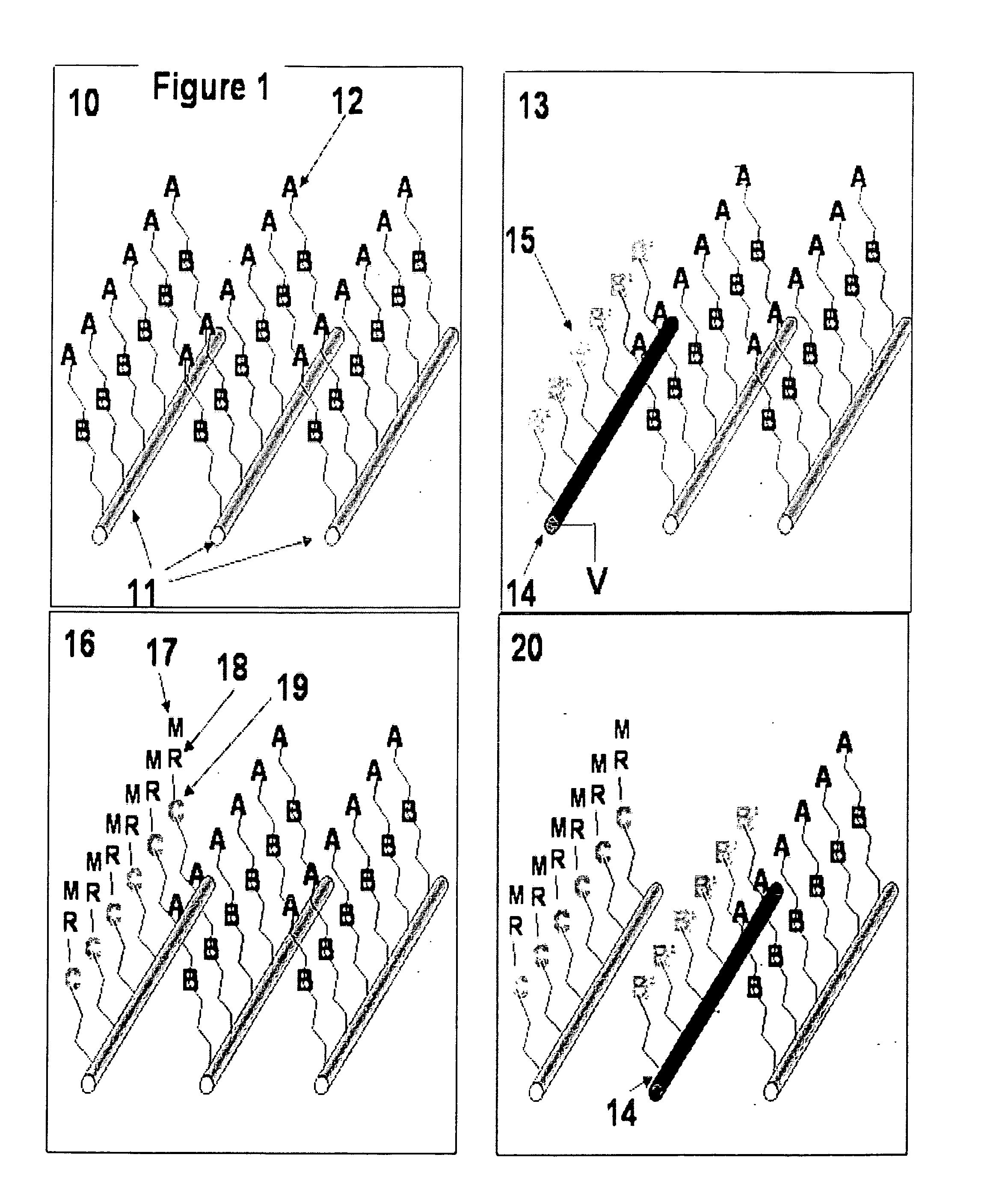
Electrochemical method and resulting structures for attaching molecular and biomolecular structures to semiconductor micro and nanostructures
a technology of molecular and biomolecular structures and electrochemical methods, which is applied in the field of micro or nanostructures, can solve the problems of limited device density within the circuit of devices that can be coated with different molecules, and achieve the effect of a wider range of applicability
- Summary
- Abstract
- Description
- Claims
- Application Information
AI Technical Summary
Benefits of technology
Problems solved by technology
Method used
Image

Examples
examples
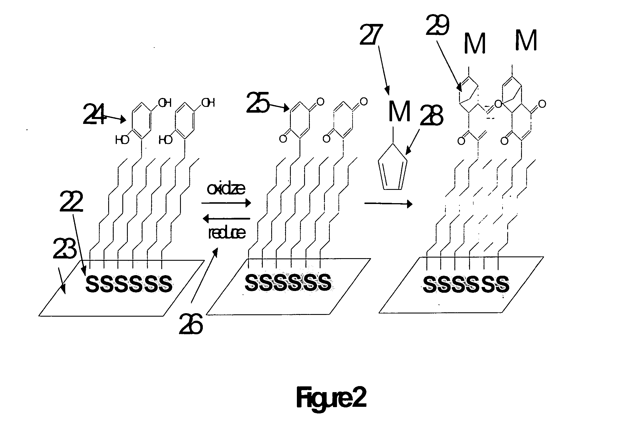
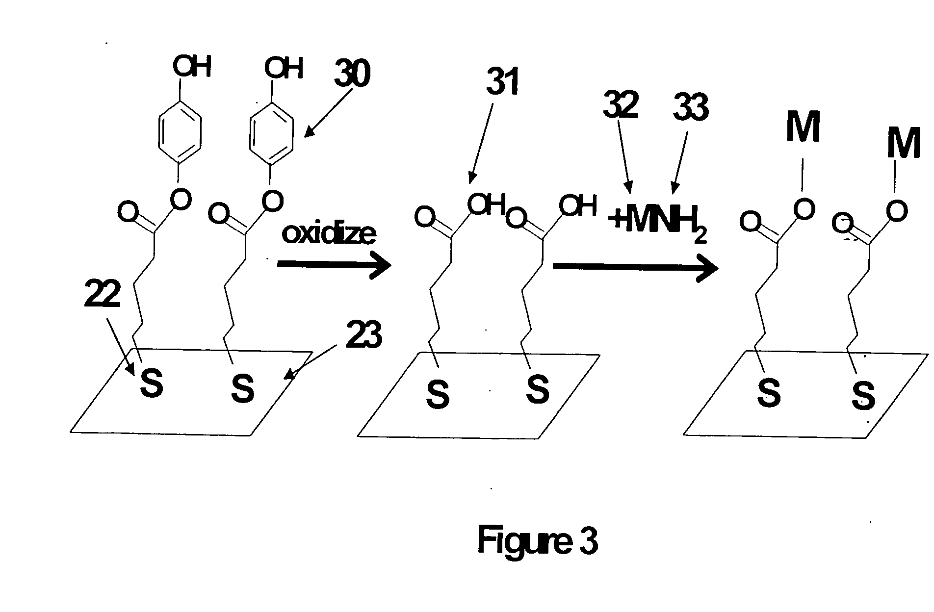
[0088] To prove the principle and demonstrate aspects of the present invention, we performed certain experiments to fabricate nanostructures with molecular probes using electrochemical reactions. Completed nanostructures with molecular probes were evaluated and tested. These experiments, however, are merely examples and should not unduly limit the scope of the claims herein. One of ordinary skill in the art would recognize many variations, modifications, and alternatives.
[0089] In FIGS. 6, 7, 8 and 9, we present an experimental approach and accompanying experimental data demonstrating aspects of the present invention. The experimental data and approach are merely examples and should not unduly limit the scope of the claims herein. One of ordinary skill in the art would recognize many variations, modifications, and alternatives. Certain details of these experiments have been provided below.
[0090] Several silicon wires were patterned on top of a 150 micrometer thick SiO2 coated sili...
PUM
| Property | Measurement | Unit |
|---|---|---|
| diameter | aaaaa | aaaaa |
| diameters | aaaaa | aaaaa |
| diameter | aaaaa | aaaaa |
Abstract
Description
Claims
Application Information