

Rinse solution and methods for forming and cleaning a semiconductor device
a technology for cleaning and semiconductor devices, applied in the direction of cleaning using liquids, instruments, photomechanical equipment, etc., can solve the problems of affecting the cleaning effect,
- Summary
- Abstract
- Description
- Claims
- Application Information
AI Technical Summary
Benefits of technology
Problems solved by technology
Method used
Image

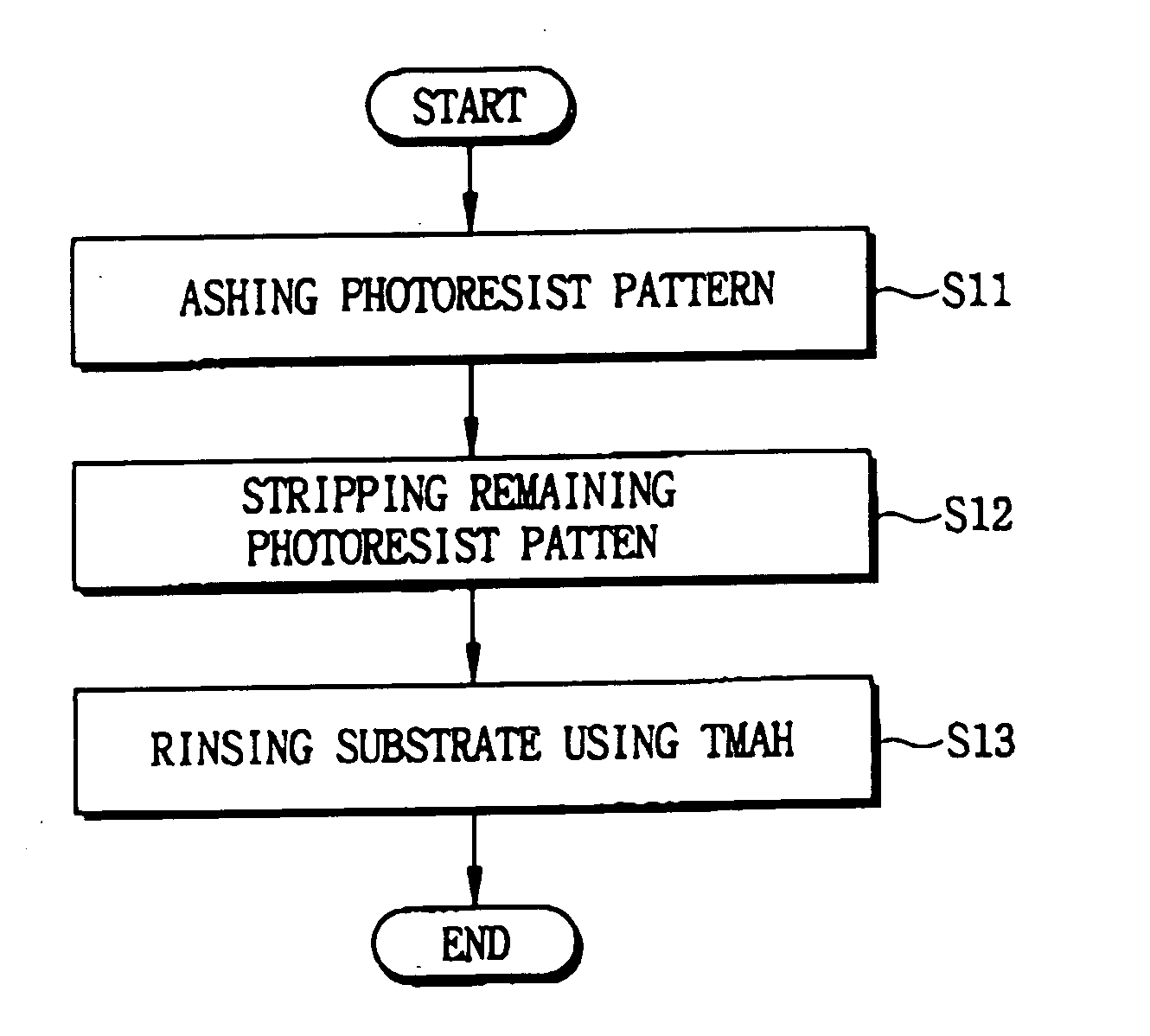
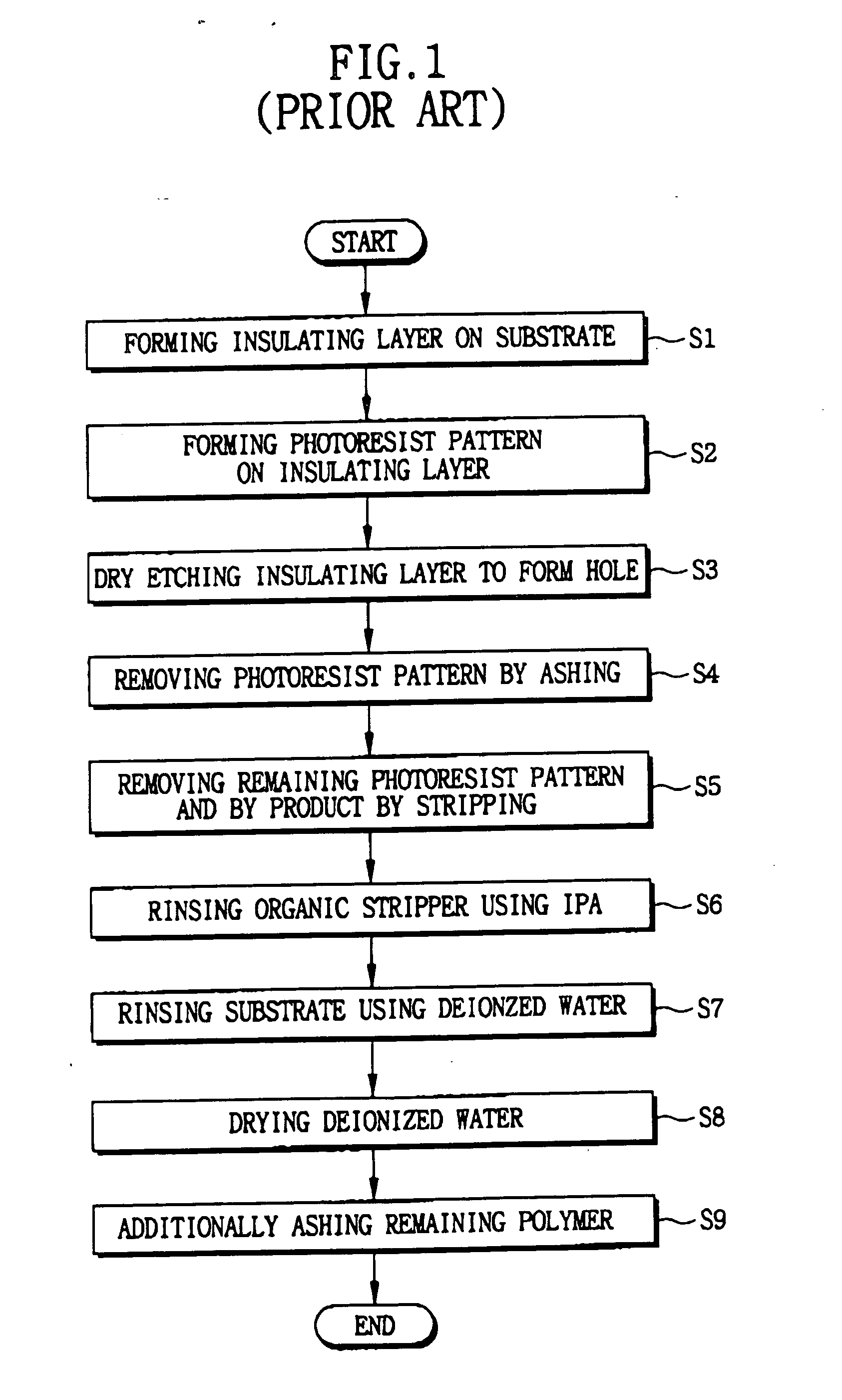
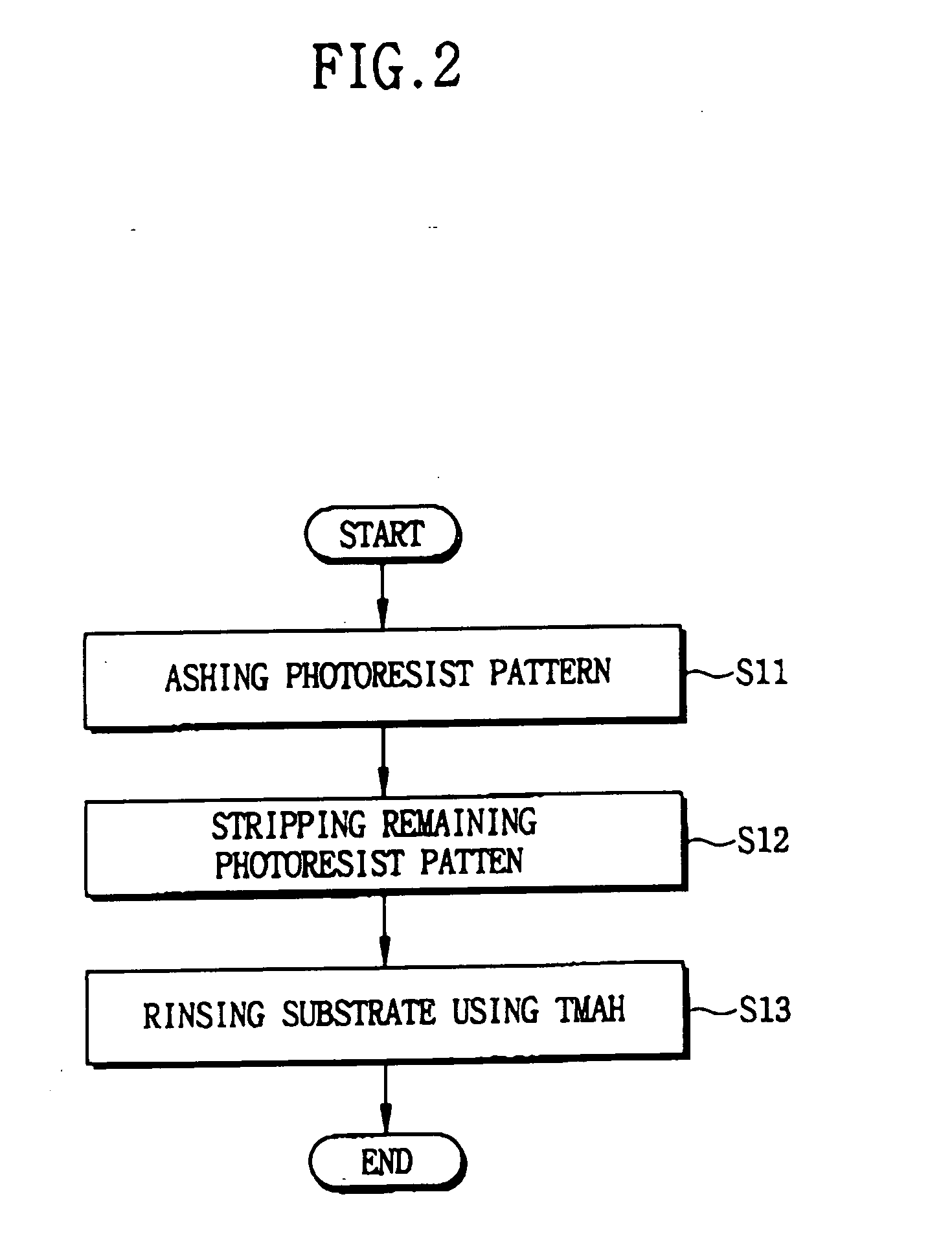
Examples
Embodiment Construction
[0027] The present invention now will be described more fully hereinafter with reference to the accompanying drawings, in which exemplary embodiments of the invention are shown. It should be understood, however, that exemplary embodiments of the present invention described herein can be modified in form and detail without departing from the spirit and scope of the invention. Accordingly, the exemplary embodiments described herein are provided by way of example and not of limitation, and the scope of the present invention is not restricted to the particular embodiments described herein. Like numbers refer to similar or identical elements throughout.
[0028] In particular, the relative thicknesses and positioning of layers or regions may be reduced or exaggerated for clarity. Further, a layer is considered as being formed “on” another layer or a substrate when formed either directly on the referenced layer or the substrate or formed on other layers or patterns overlaying the referenced...
PUM
| Property | Measurement | Unit |
|---|---|---|
| temperature | aaaaa | aaaaa |
| temperature | aaaaa | aaaaa |
| weight | aaaaa | aaaaa |
Abstract
Description
Claims
Application Information