

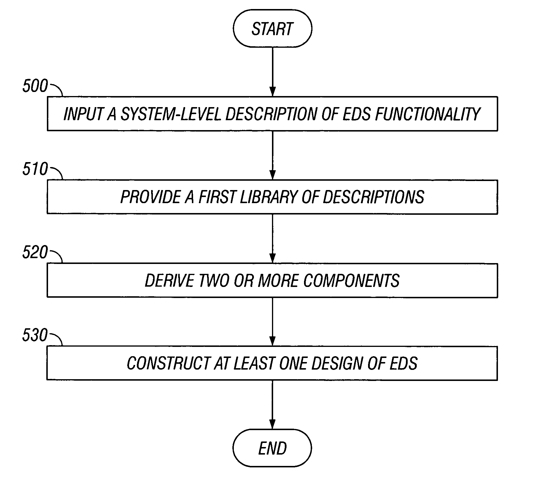
Design method for essentially digital systems and components thereof and essentially digital systems made in accordance with the method
a technology of essentially digital systems and components, applied in the direction of cad techniques, multi-objective optimisation, instruments, etc., can solve problems such as systematic breakage or movemen
- Summary
- Abstract
- Description
- Claims
- Application Information
AI Technical Summary
Benefits of technology
Problems solved by technology
Method used
Image

Examples
Embodiment Construction
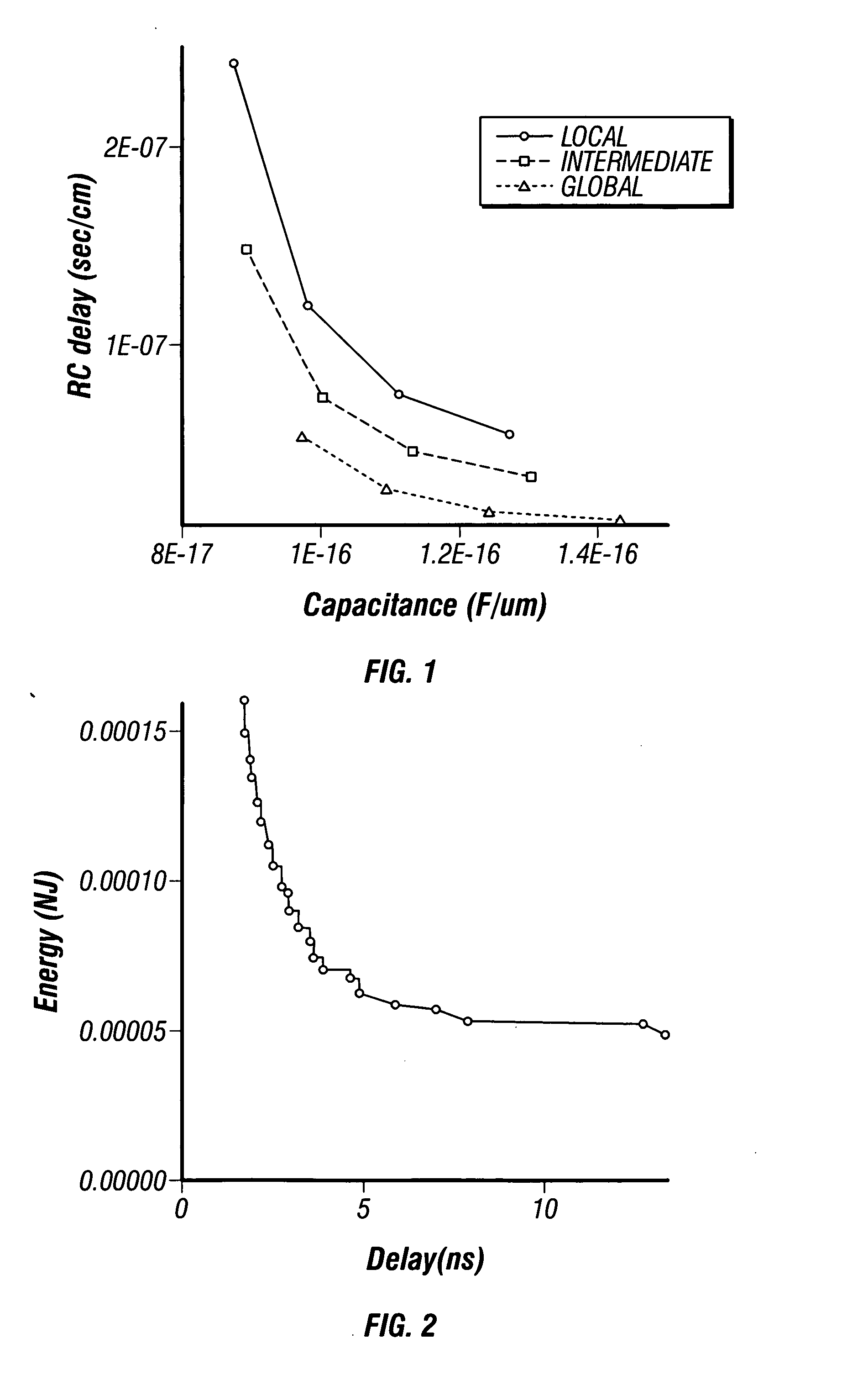
In past and present technology nodes the power consumption of the chips was heavily dominated by the consumption in the transistors. Delay was also contributed mainly by the logic parts of the chip. But as feature size scales down, transistors become smaller and smaller. The result is that they become faster and less power consuming. Interconnections on the other hand cannot benefit from feature size scaling. In every technology node the pitch is decreased, making interconnect wires smaller and forcing them to be closer to each other. The smaller cross-sections of the wires that are necessary inevitably lead to a larger resistance of the line, while having very dense wiring on-chip increases the trans-capacitance of these wires. These effects create a number of problems, such as problems to cross long distances at the high clock frequency, cross-talk, increased power consumption and so on.
From Davis et al. [5] it becomes clear that the trend is that interconnect delay will increa...
PUM
 Abstract
Description
Claims
Application Information