Semiconductor device

a technology of semiconductor devices and semiconductors, applied in semiconductor devices, semiconductor/solid-state device details, printed circuits, etc., can solve the problems of difficult distribution of wires in wire bonding, difficult to keep the height of the package at a certain level, and difficult to reduce the cost. , to achieve the effect of high density in packaging, enhanced reliability, and higher function

Inactive Publication Date: 2005-02-24
RENESAS ELECTRONICS CORP
View PDF10 Cites 25 Cited by
  • Summary
  • Abstract
  • Description
  • Claims
  • Application Information

AI Technical Summary

Benefits of technology

[0009] It is an object of the present invention to provide a semiconductor device that is capable of attaining a high-density in packaging.
[0010] It is another object of the present invention to provide a semiconductor device that is capable of enhanced the reliability.
[0011] It is a further object of the present invention to provide a semiconductor device that is capable of attaining higher functions.

Problems solved by technology

As a result of studies directed to stacked type and small-sized, high-function semiconductor devices, the following problems were discovered.
In this connection, for the attainment of higher functions in a small-sized BGA (Ball Grid Array), if the number of semiconductor chips is increased, there arises the problem that a reduction of the cost is difficult due to the influence of yield in sorting chips.
In a system in a package formed as a combination of logic / ASIC and memory, there arises the problem that the distribution of wires in wire bonding is difficult due to the positional relation between common pins and independent pins.
Further, in wire bonding in a small-size and thin package, it is difficult to keep the package height at a certain level due to the influence of loop height.

Method used


Image

  • Semiconductor device
  • Semiconductor device
  • Semiconductor device

Examples


first embodiment

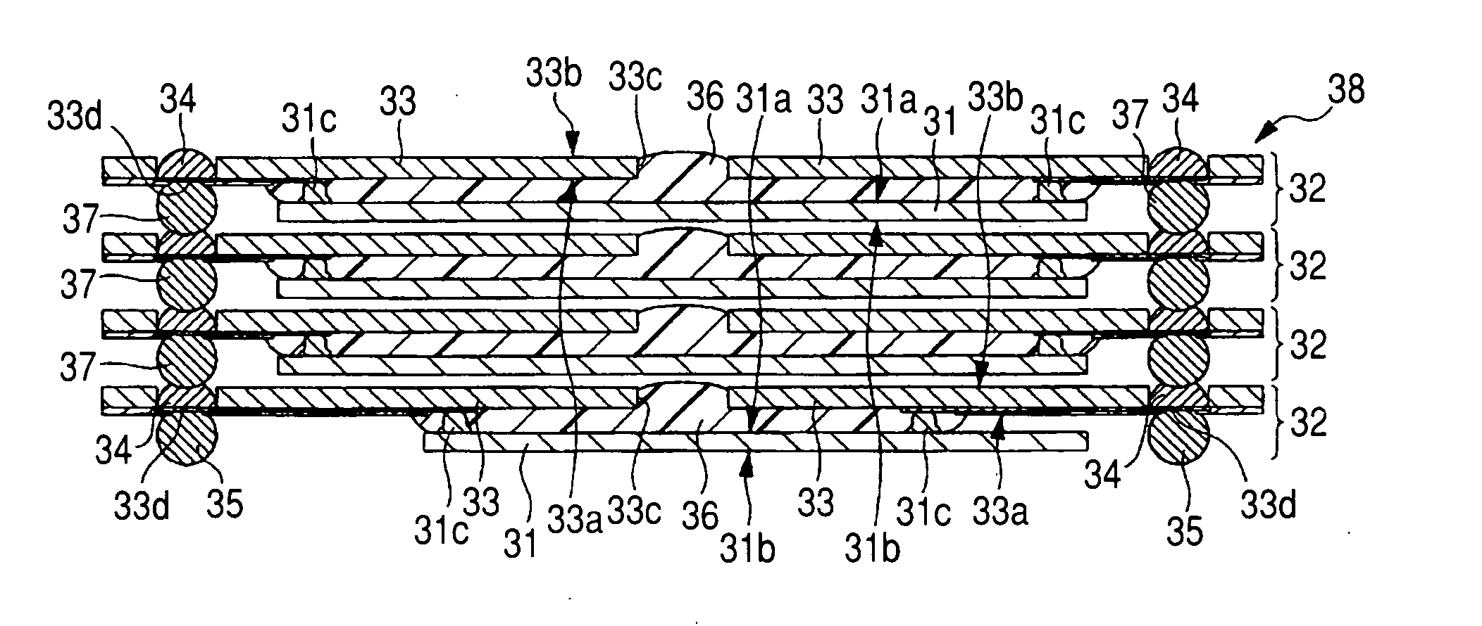
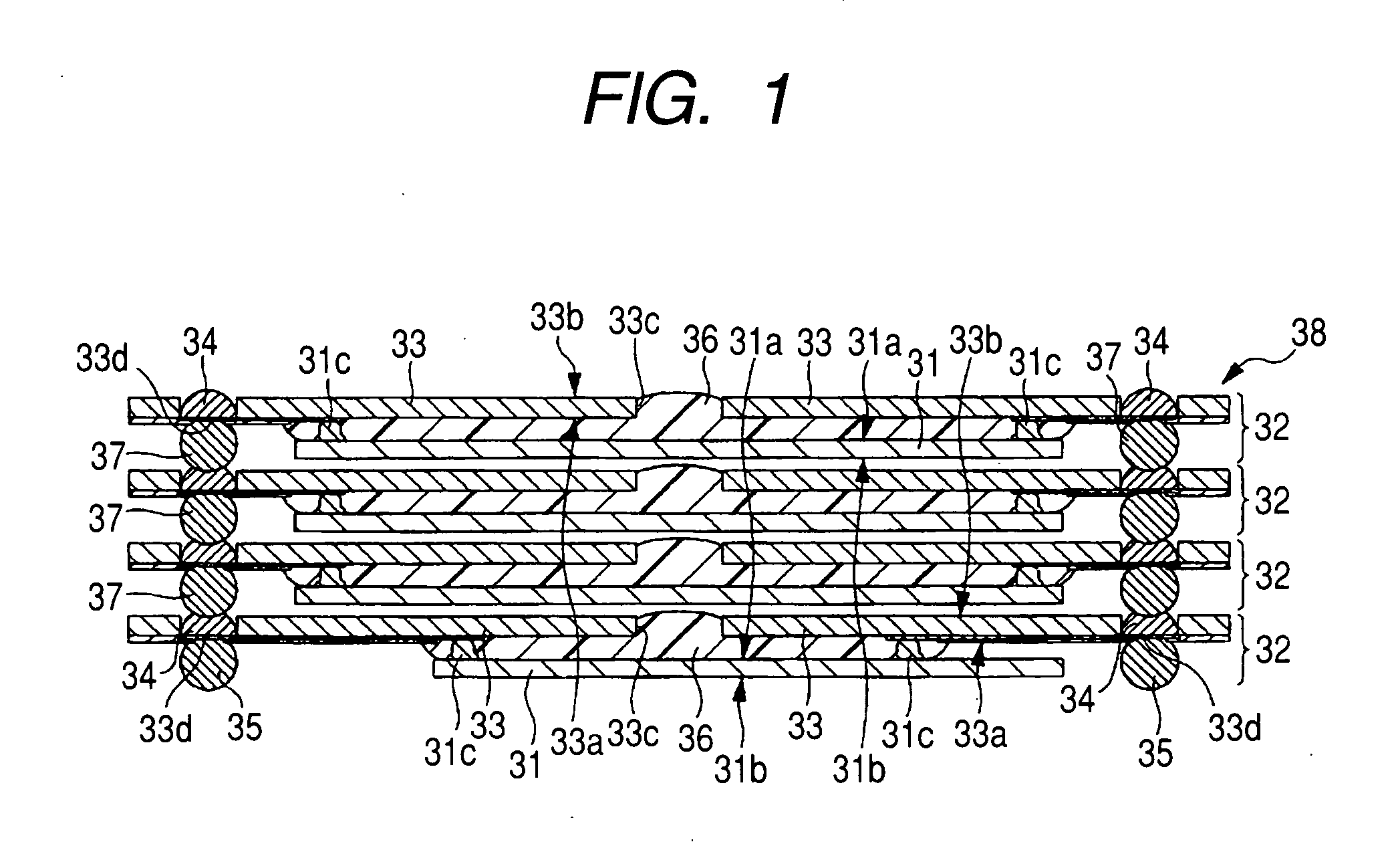
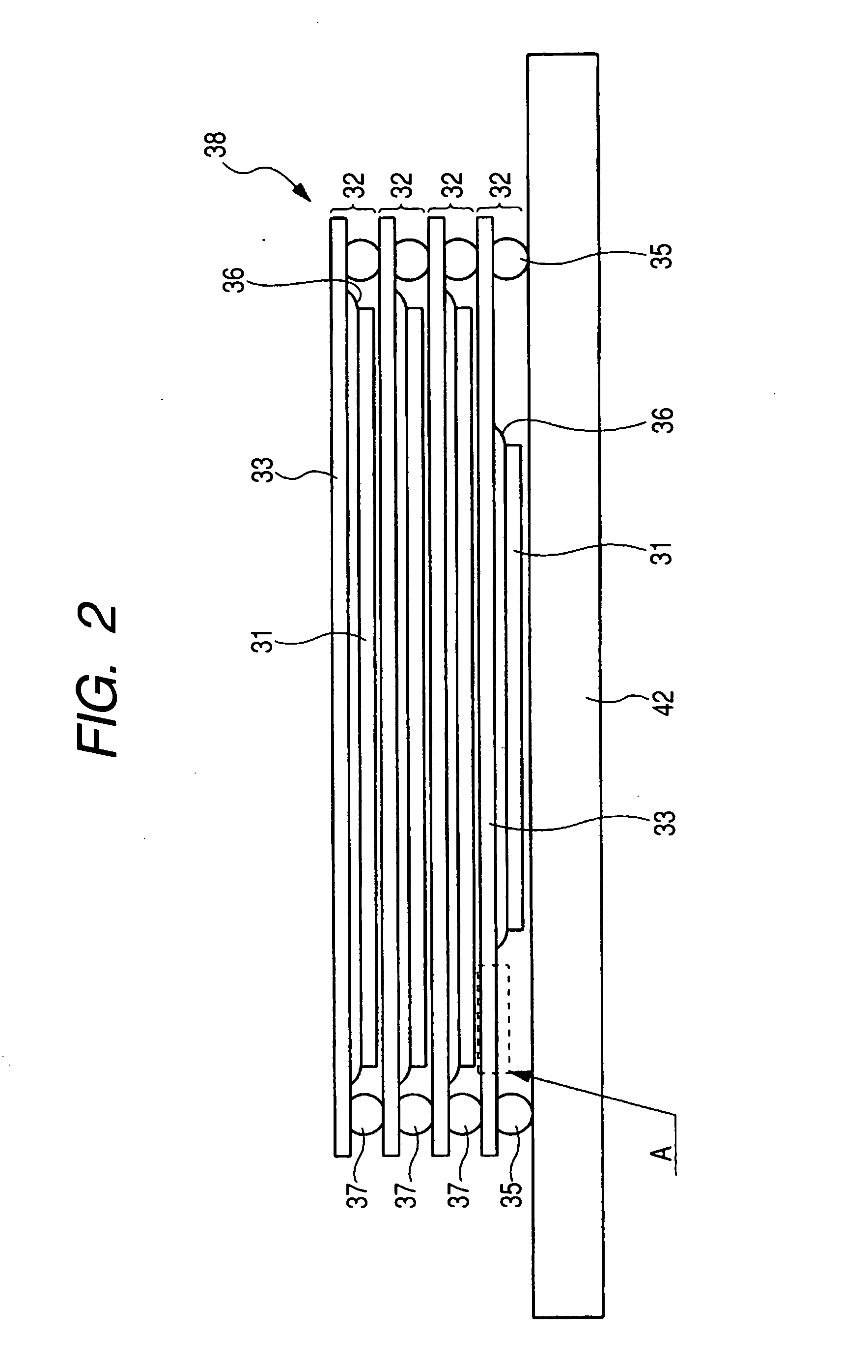
[0066]FIG. 1 is a sectional view showing a structural example of a semiconductor device according to a first embodiment of the present invention; FIG. 2 is a side view showing an example of a mounting structure for mounting the semiconductor device illustrated in FIG. 1 onto a mounting substrate; FIG. 3 is a side view showing the structure of a semiconductor device according to a modification of the first embodiment; FIG. 4 is a bottom view showing an example of a land array on a memory chip mounting wiring substrate in the semiconductor device illustrated in FIG. 3; and FIG. 5 is a bottom view showing an example of a land array on a logic chip mounting wiring substrate in the semiconductor device illustrated in FIG. 3.

[0067] The semiconductor device of this first embodiment is in the form of a stacked type package 38 wherein a semiconductor chip 31 is flip-chip-connected to a wiring substrate and plural such structures are stacked.

[0068] More specifically, the semiconductor devic...

second embodiment

[0098]FIG. 6 is a sectional view showing a structural example of a semiconductor device according to a second embodiment of the present invention; FIG. 7 is a plan view showing an example of the distribution of wires in a first layer in a bottom-stage wiring substrate in the semiconductor device illustrated in FIG. 6; FIG. 8 is a plan view showing an example of the distribution of wires in a second layer in the bottom-stage wiring substrate in the semiconductor device illustrated in FIG. 6; FIG. 9 is a plan view showing an example of the distribution of wires in a third layer in the bottom-stage wiring substrate in the semiconductor device illustrated in FIG. 6; FIG. 10 is a plan view showing an example of the distribution of wires in a fourth layer in the bottom-stage wiring substrate in the semiconductor device illustrated in FIG. 6; FIG. 11 is a plan view showing an example of the distribution of wires in a top-stage wiring substrate in a semiconductor device of a six-layer struc...

third embodiment

[0136]FIG. 16 is a sectional view showing a structural example of a semiconductor device according to a third embodiment of the present invention; FIG. 17 is a sectional view showing an example of an under-fill sealing method used in assembling the semiconductor device illustrated in FIG. 16; FIG. 18 is a partial perspective view showing the under-fill sealing method illustrated in FIG. 17; FIG. 19 is a manufacturing process flow chart showing an example of a procedure for assembling the semiconductor device illustrated in FIG. 16; FIG. 20 is a plan view showing an example of a state of resin diffusion produced by the under-fill sealing method illustrated in FIG. 18, FIG. 21 is a plan view showing a state of resin diffusion by the under-fill sealing method in case of using a wiring substrate according to a modification of the third embodiment; FIG. 22 is a plan view showing a state of resin diffusion produced by the under-fill sealing method in case of using a wiring substrate accor...


PUM


Abstract

For high density packaging of a semiconductor device, the semiconductor device has a multi-layer substrate, a first-stage chip connected electrically to the multi-layer substrate, other package substrates stacked in three stages on the multi-layer substrate and each connected to an underlying wiring substrate through solder balls, second-, third- and fourth-stage chips electrically connected respectively to the other package substrates, and solder balls provided on the bottom multi-layer substrate. The number of wiring layers in the bottom multi-layer substrate which has a logic chip is larger than that in the package substrates which have memory chips, whereby the semiconductor device can have a wiring layer not used for distribution of wires to the solder balls and wiring lines in the wiring layer can be used for the mounting of another semiconductor element or a passive component to attain high density packaging of the semiconductor device as a stacked type package.

Description

CROSS-REFERENCE TO RELATED APPLICATION [0001] The present application claims priority from Japanese patent applications JP 2003-199467, filed on Jul. 18, 2003, JP 2003-159305, filed on Jun. 4, 2003 and JP 2003-175792, filed on Jun. 20, 2003, the content of each of which is hereby incorporated by reference into this application. BACKGROUND OF THE INVENTION [0002] The present invention relates to a semiconductor device. More particularly, the present invention is concerned with a technique that is applicable effectively to a semiconductor device having a stacked structure formed of plural wiring substrates. [0003] In conventional stacked type semiconductor devices, two or more semiconductor devices, each having a semiconductor element mounted in a recess formed in an insulating substrate, are stacked on an external substrate; and, the semiconductor devices themselves are made thin, so that various types of semiconductor elements can be mounted in three dimensions (see, for example, Pa...

Claims


Application Information

Patent Timeline
Patent Type & Authority Applications(United States)
IPC IPC(8): H01L21/56H01L23/31H01L23/12H01L25/10H05K1/00
CPCH01L21/563H01L23/3128H01L2225/1058H01L2225/1023H01L2924/3511H01L2224/32225H01L2924/01019H01L2924/01006H01L2924/1532H01L2924/15311H01L2924/15192H01L2924/15174H01L2924/15151H01L2924/1433H01L2924/14H01L24/28H01L25/105H01L2224/16225H01L2224/73203H01L2224/73204H01L2224/83102H01L2224/92125H01L2924/01002H01L2924/01005H01L2924/01015H01L2924/01033H01L2924/0105H01L2924/01075H01L2924/01078H01L2924/01079H01L2924/01082H01L2924/00012H01L2924/00H01L2224/05571H01L2224/05573H01L23/12H05K1/00
Inventor KIKUCHI, TAKASHIKIMOTO, RYOSUKEKAWAKUBO, HIROSHIMIWA, TAKASHIIMURA, CHIKAKONISHITA, TAKAFUMIKOYAMA, HIROSHISHIBAMOTO, MASANORIKAWAKAMI, MASARU
Owner RENESAS ELECTRONICS CORP
Why Eureka
Try Eureka