Construction structures and manufacturing processes for integrated circuit wafer probe card assemblies

a technology of integrated circuit wafer and assembly structure, which is applied in the direction of printed element electric connection formation, coupling device connection, instruments, etc., can solve the problems of limited pitch, small pad pitch, high clock frequency, and inability to use tungsten needle probes, so as to reduce assembly manufacturing cost and manufacturing time, and extend mechanical compliance. , the effect of high speed testing

Inactive Publication Date: 2005-02-24
ADVANTEST SINGAPORE PTE LTD
View PDF1 Cites 50 Cited by
  • Summary
  • Abstract
  • Description
  • Claims
  • Application Information

AI Technical Summary

Benefits of technology

[0023] Several embodiments of integrated circuit probe card assemblies are disclosed, which extend the mechanical compliance of both MEMS and thin-film fabricated probes, such that these types of spring probe structures can be used to test one or more integrated circuits on a semiconductor wafer. Several embodiments of probe card assemblies are disclosed, which provide tight signal pad pitch and compliance, preferably enabling the parallel testing or burn-in of multiple ICs, using commercial wafer probing equipment. In some preferred embodiments, the probe card assembly structures include separable standard electrical connector components, which reduces assembly manufacturing cost and manufacturing time. These structures and assemblies enable high speed testing of IC's in wafer form, as well as high density substrates. The probes preferably include mechanical protection for both the integrated circuits and the MEMS or thin film fabricated spring tips. Interleaved spring probe tip designs are defined which allow multiple probe contacts on very small integrated circuit pads. The shapes of probe tips are preferably defined to control the depth of probe tip penetration between a probe spring and a pad or trace on an integrated circuit device. Improved protective coating techniques for spring probes are also disclosed, offering increased quality and extended useful service lives for probe card assemblies.

Problems solved by technology

However, advanced semiconductor technologies often require higher pin counts, smaller pad pitches, and higher clock frequencies, which are not possible with tungsten needle probes.
While emerging technologies have provided spring probes for different probing applications, most probes have inherent limitations, such as limited pitch, limited pin count, varying levels of flexibility, limited probe tip geometries, limitations of materials, and high costs of fabrication.
As a result, there is even greater component density but without interference of wire bonds one with the other, this factor of interference being the previous limiting factor in achieving high component density networks in a multi-layer ceramic package”.
While the contact tip structures disclosed by B. Eldridge et al. provide resilient contact structures, the structures are each individually mounted onto bond pads on semiconductor dies, requiring complex and costly fabrication.
As well, the contact tip structures are fabricated from wire, which often limits the resulting geometry for the tips of the contacts.
Furthermore, such contact tip structures have not been able to meet the needs of small pitch applications (e.g. typically on the order of 50 μm spacing for a peripheral probe card, or on the order of 75 μm spacing for an area array).
While the photolithography patterned springs, as disclosed by Smith et al., are capable of satisfying many IC probing needs, the springs are small, and provide little vertical compliance to handle the planarity compliance needed in the reliable operation of many current IC prober systems.
Furthermore, no one has taught a way to interconnect such a probe containing up to several thousand pins to a tester, while effectively dealing with planarity requirements.

Method used


Image

  • Construction structures and manufacturing processes for integrated circuit wafer probe card assemblies
  • Construction structures and manufacturing processes for integrated circuit wafer probe card assemblies
  • Construction structures and manufacturing processes for integrated circuit wafer probe card assemblies

Examples


Embodiment Construction

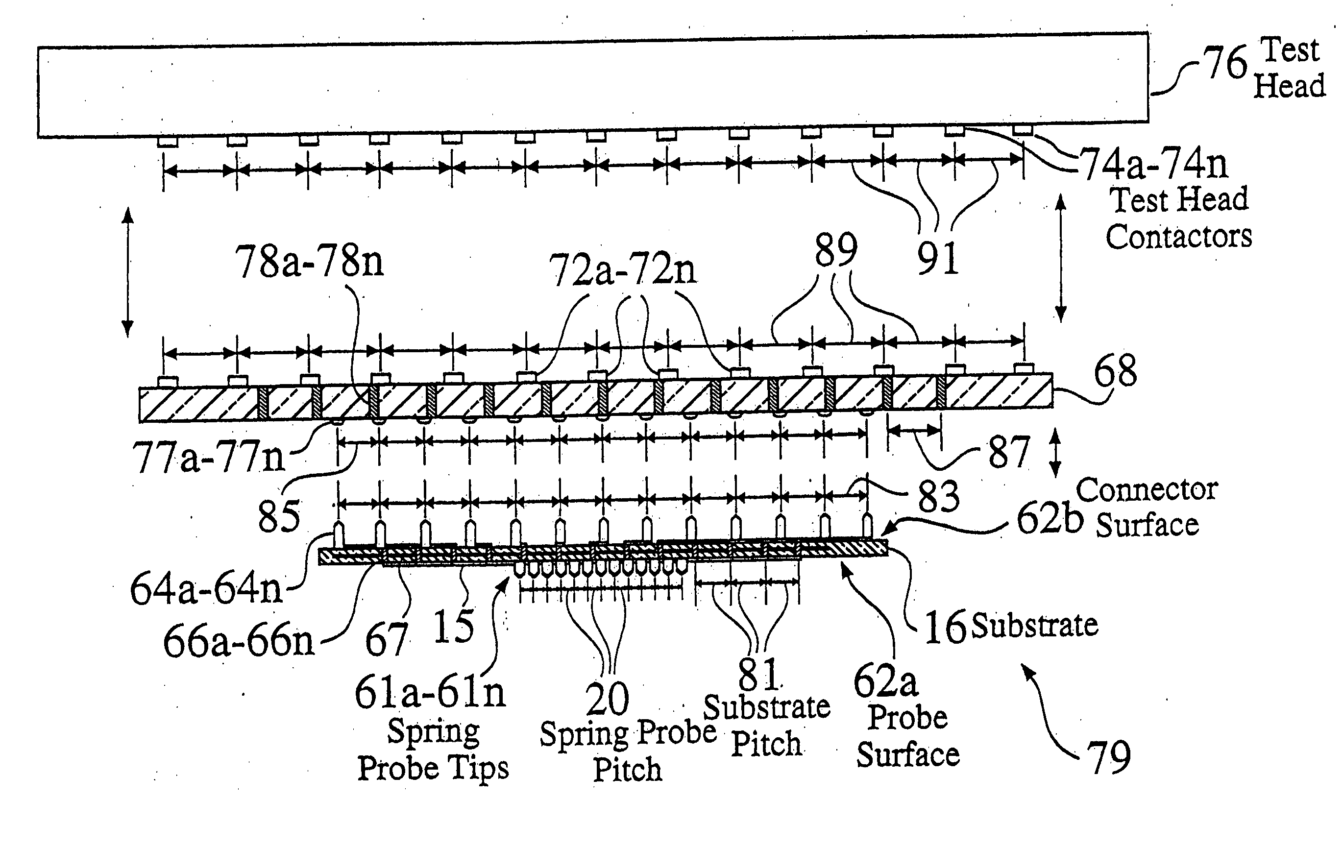
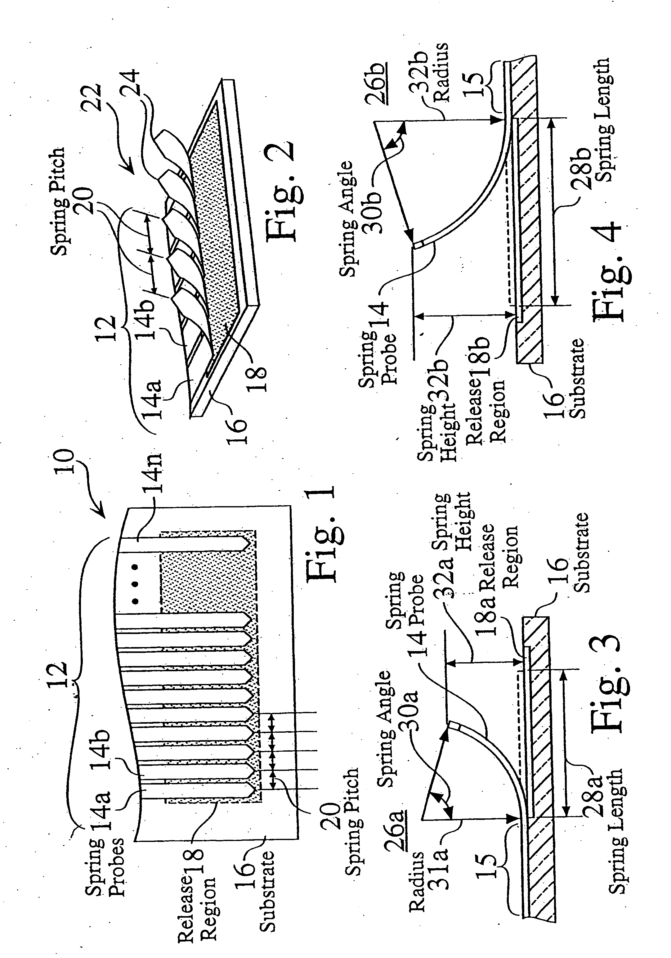
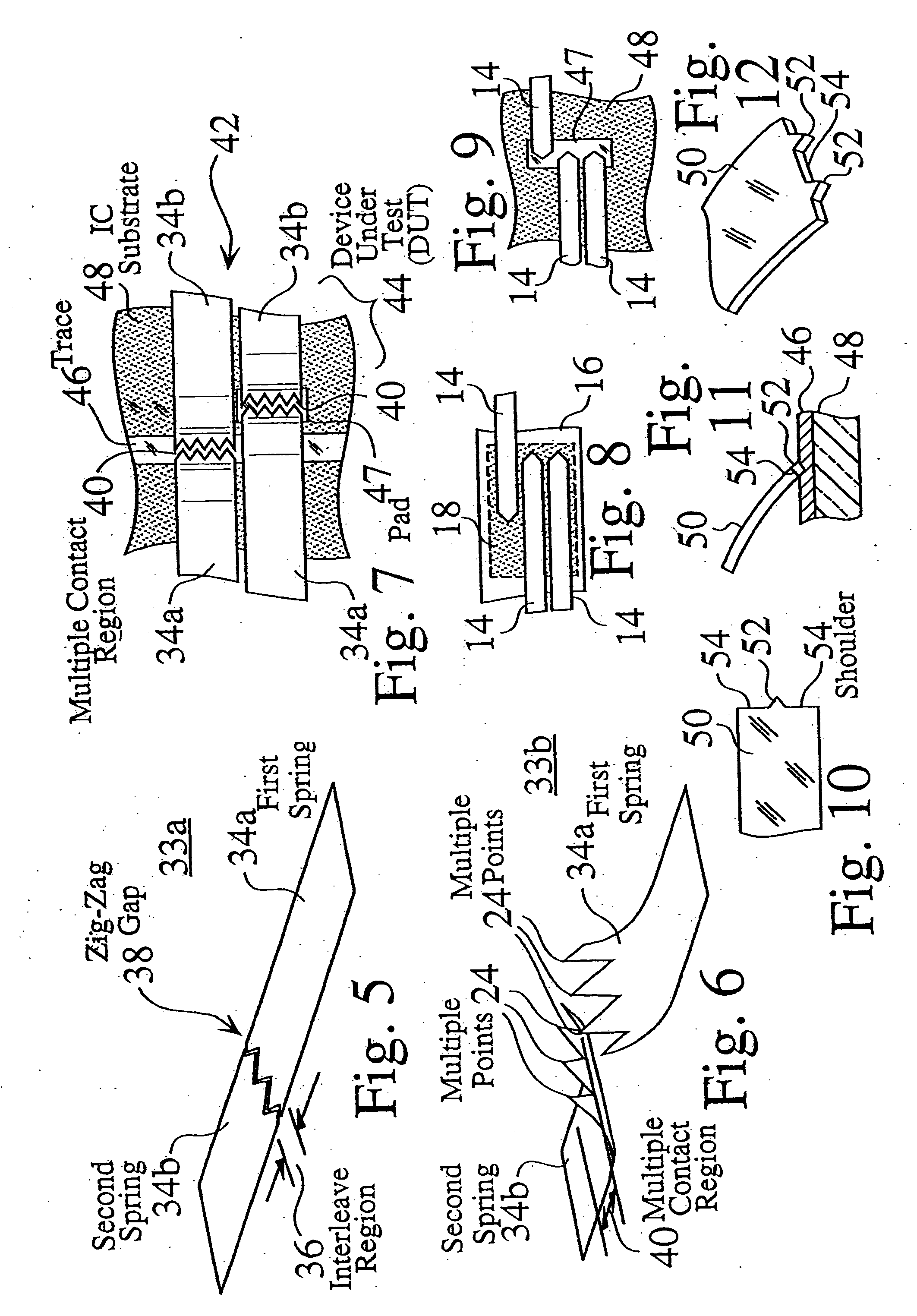
[0071]FIG. 1 is a plan view 10 of a linear array 12 of photolithographically patterned springs 14a-14n, prior to release from a substrate 16. The conductive springs 14a-14n are typically formed on the substrate layer 16, by two or more successive layers 17, (e.g. such as 17a,17b in FIG. 47) of deposited metal, such as through low and high energy plasma deposition processes, followed by photolithographic patterning, as is widely known in the semiconductor industry. The successive layers 17a,17b have different inherent levels of stress. The release regions 18 of the substrate 16 are then processed by undercut etching, whereby portions of the spring contacts 14a-14n located over the release region 18, are released from the substrate 16 and extend (i.e. bend) away from the substrate 16, as a result of the inherent stresses between the deposited metallic layers 17a,17b. Fixed regions 15 (FIG. 3, FIG. 4) of the deposited metal traces remain affixed to the substrate 16, and are typically u...


PUM


Abstract

Several embodiments of integrated circuit probe card assemblies are disclosed, which extend the mechanical compliance of both MEMS and thin-film fabricated probes, such that these types of spring probe structures can be used to test one or more integrated circuits on a semiconductor wafer. Several embodiments of probe card assemblies, which provide tight signal pad pitch compliance and/or enable high levels of parallel testing in commercial wafer probing equipment, are disclosed. In some preferred embodiments, the probe card assembly structures include separable standard components, which reduce assembly manufacturing cost and manufacturing time. These structures and assemblies enable high speed testing in wafer form. The probes also have built in mechanical protection for both the integrated circuits and the MEMS or thin film fabricated spring tips and probe layout structures on substrates. Interleaved spring probe tip designs are defined which allow multiple probe contacts on very small integrated circuit pads. The shapes of probe tips are preferably defined to control the depth of probe tip penetration between a probe spring and a pad or trace on an integrated circuit device. Improved protective coating techniques for spring probes are also disclosed, offering increased reliability and extended useful service lives for probe card assemblies.

Description

CROSS-REFERENCE TO RELATED APPLICATIONS [0001] This application is a divisional of U.S. Ser. No. 10 / 094,370 filed Mar. 8, 2002 (Attorney Docket No. NNEX0003D), and U.S. Ser. No. 09 / 980,040 filed Nov. 27, 2001 (Attorney Docket No. NNEX0003), and claims priority of International Patent Application No. PCT / US00 / 21012, filed 28 Jul. 2000, and U.S. Provisional Application 60 / 146,241, filed 28 Jul. 1999, all of which are incorporated herein in their entirety by this reference thereto.FIELD OF THE INVENTION [0002] The invention relates to the field of probe card assembly systems. More particularly, the invention relates to improvements in photolithography-patterned spring contacts and enhanced probe card assemblies having photolithography-patterned spring contacts for use in the testing or burn-in of integrated circuits. BACKGROUND OF THE INVENTION [0003] In conventional integrated circuit (IC) wafer probe cards, electrical contacts between the probe card and an integrated circuit wafer ar...

Claims


Application Information

Patent Timeline
Patent Type & Authority Applications(United States)
IPC IPC(8): G01R1/073G01R3/00G01R31/28H05K3/40H05K7/10
CPCG01R1/07371G01R1/07378G01R3/00H05K7/1061G01R31/2887H05K3/4092G01R31/2886
Inventor MOK, SAMMYCHONG, FU CHIUNG
Owner ADVANTEST SINGAPORE PTE LTD
Why Eureka
Try Eureka