Method, system, and article of manufacture for implementing metal-fill with power or ground connection

a technology of power or ground connection and metal filling, applied in the field of integrated circuit design and manufacture, can solve the problems of reducing affecting the process of cmp, and bumps in the finished chip, so as to reduce local step height, reduce yield and impact circuit performance, and reduce the variation of layout pattern dependent dielectric thickness

Inactive Publication Date: 2005-02-24
CADENCE DESIGN SYST INC
View PDF40 Cites 37 Cited by
  • Summary
  • Abstract
  • Description
  • Claims
  • Application Information

AI Technical Summary

Problems solved by technology

However, CMP processes have been hampered by layout pattern dependent variation in the inter-level dielectric (ILD) thickness which can reduce yield and impact circuit performance.
Otherwise, an insufficient amount of metal may cause bumps to exist in the finished chip.
However, too much metal may cause dishing to occur.
In some cases, the selected metal-fill pattern may contain too much metal, causing the new layout to exceed maximum metal percentages as specified by the manufacturer.
In other cases, the metal-fill pattern may contain too little metal, causing the new layout to fall beneath specified minimum metal percentages.
This trial and error approach can be costly and inefficient, particularly if the iterative steps of the process must be manually performed.
Moreover, as new chip designs become smaller, the required metal percentage requirements become even stricter, which may require even more passes through this process to achieve an acceptable metal percentage.

Method used


Image

  • Method, system, and article of manufacture for implementing metal-fill with power or ground connection
  • Method, system, and article of manufacture for implementing metal-fill with power or ground connection
  • Method, system, and article of manufacture for implementing metal-fill with power or ground connection

Examples


Embodiment Construction

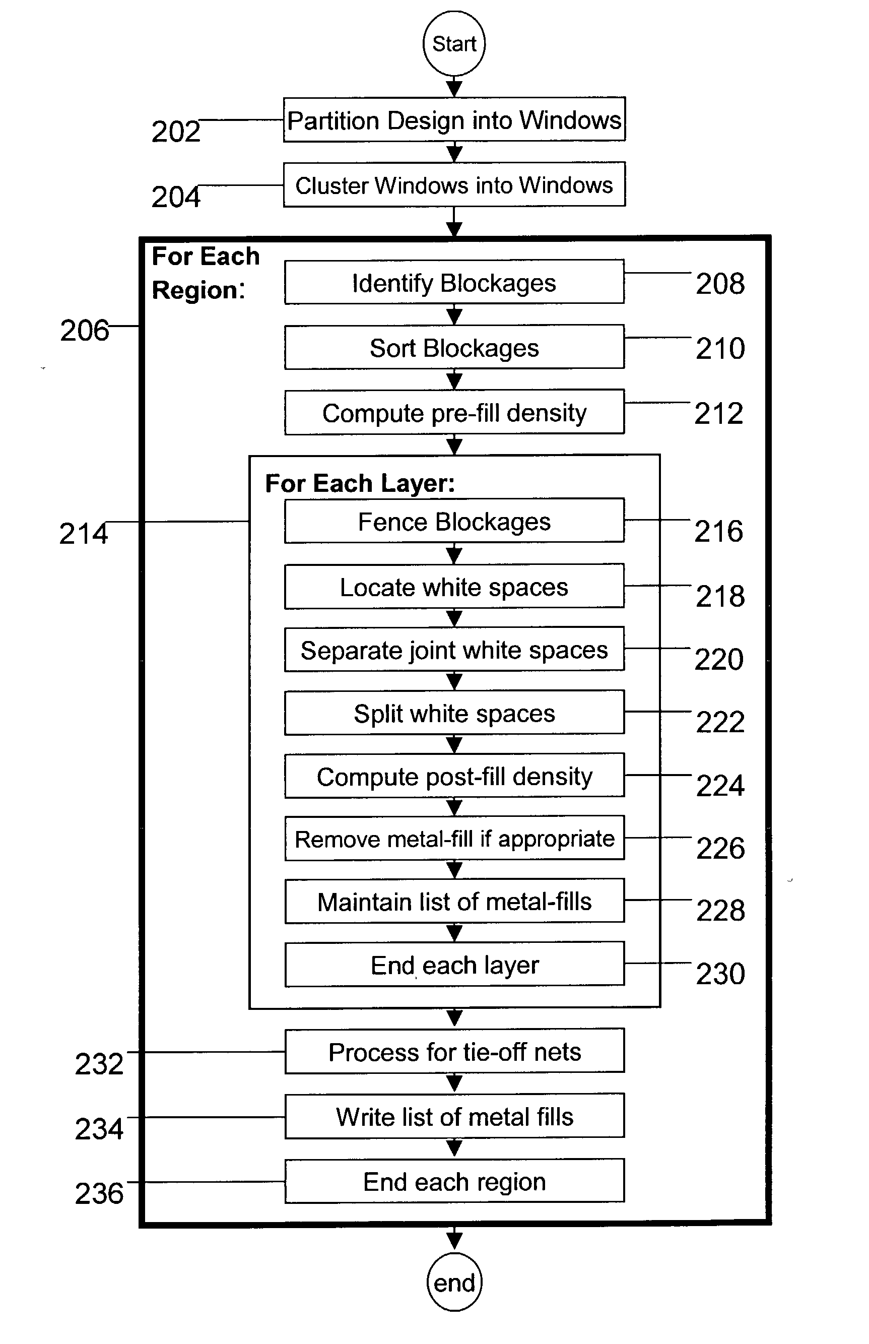
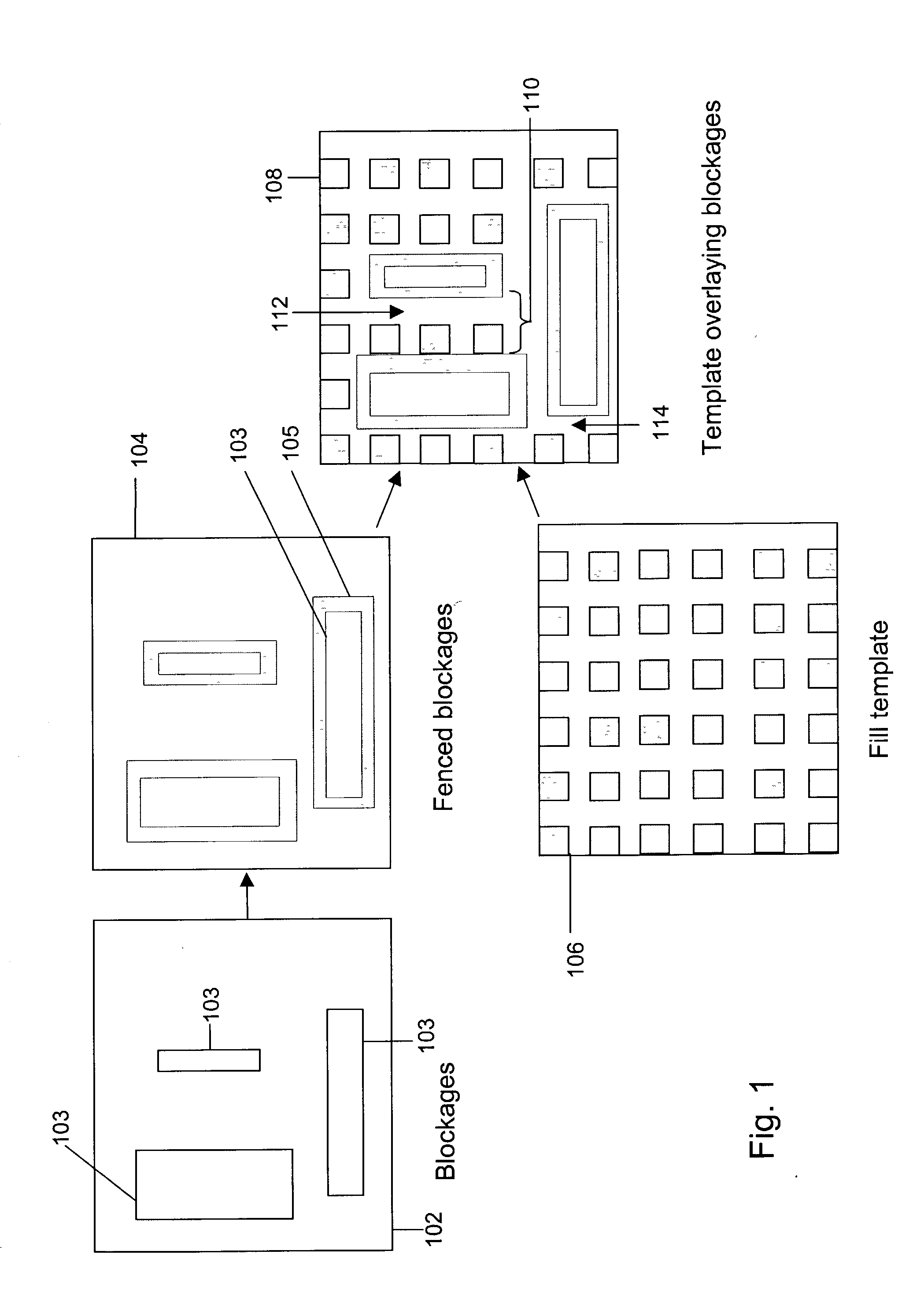
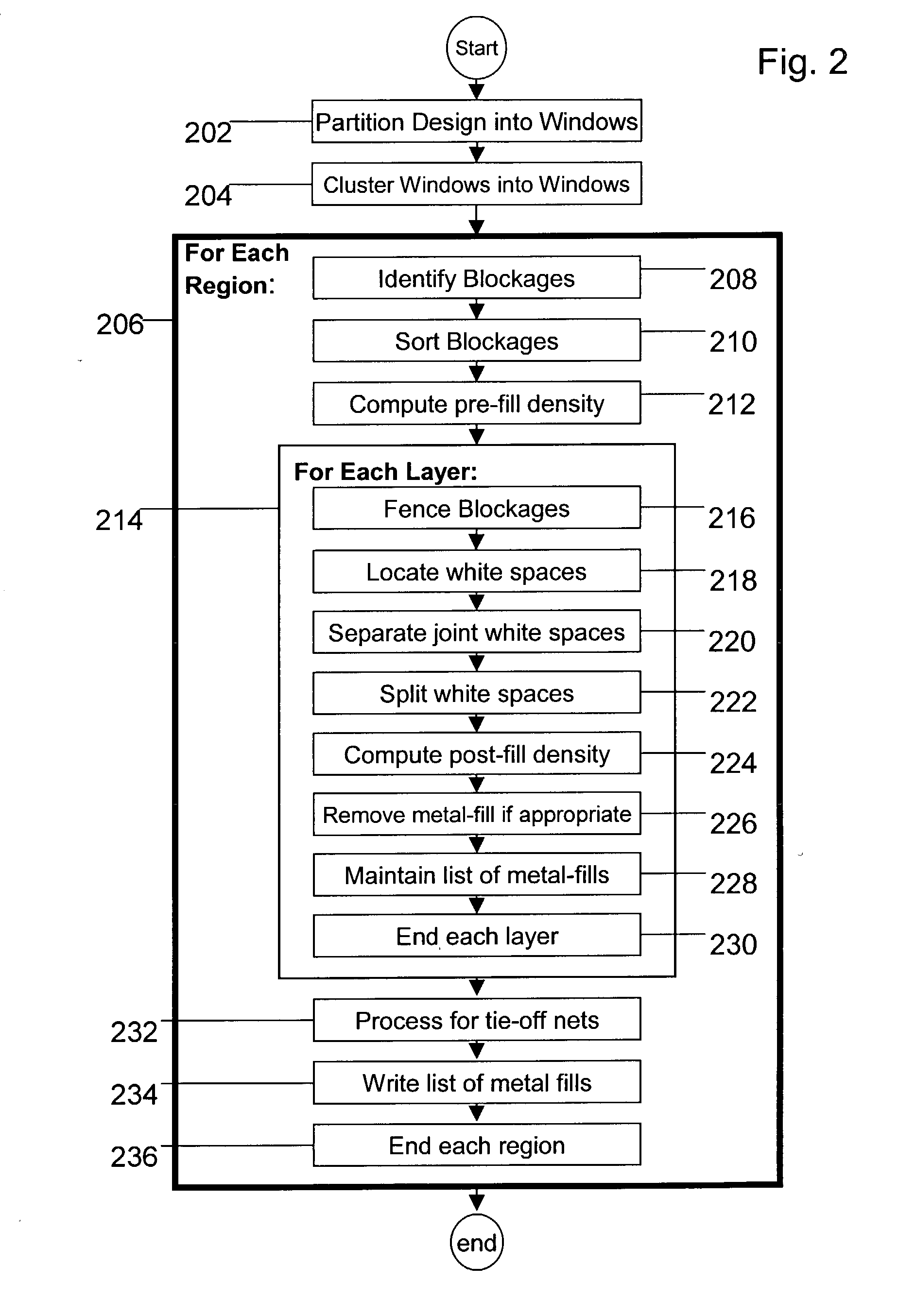
The present invention is directed to an improved method, system, and article of manufacture for implementing metal-fill for an integrated circuit. A disclosed embodiment calculates the best offset in each local area to be filled (e.g. minimum spacing from the existing metal), and dynamically adjust shape widths and different shape lengths that best fill that area. A metal-fill window will be processed in one pass, with possibly different sizes or shapes of metal-fill in the windows. An embodiment also simultaneously optimizes across multiple metal-fill windows such that that the process will not add shapes in a window that would exceed the maximum density, while attempting to make all windows match the preferred density, and meeting the minimum density.

FIG. 2 shows a flowchart of a metal-fill procedure according to an embodiment of the invention. Some example inputs to this procedure are: (a) the minimum and maximum fill width and length; (b) minimum, maximum and preferred density...


PUM


Abstract

Disclosed is a method, system, and article of manufacture for a one-pass approach for implementing metal-fill for an integrated circuit. Also disclosed is a method, system, and article of manufacture for implementing metal-fill that is coupled to a tie-off connection. An approach that is disclosed comprises a method, system, and article of manufacture for implementing metal-fill having an elongated shape that corresponds to the length of whitespace. Also disclosed is the aspect of implementing metal-fill that matches the routing direction. Yet another disclosure is an implementation of a place & route tool incorporating an integrated metal-fill mechanism.

Description

COPYRIGHT NOTICE A portion of the disclosure of this patent document contains material which is subject to copyright protection. The copyright owner has no objection to the facsimile reproduction by anyone of the patent document or the patent disclosure, as it appears in the Patent and Trademark Office patent files and records, but otherwise reserves all other copyright rights. BACKGROUND AND SUMMARY The invention relates to the design and manufacture of integrated circuits, and more particularly, to techniques, systems, and methods for implementing metal-fill patterns on an integrated circuit. In recent years, in IC manufacturing, chemical-mechanical polishing (CMP) has emerged as an important technique for planarizing dielectrics because of its effectiveness in reducing local step height and achieving a measure of global planarization not normally possible with spin-on and resist etch back techniques. However, CMP processes have been hampered by layout pattern dependent variati...

Claims


Application Information

Patent Timeline
Patent Type & Authority Applications(United States)
IPC IPC(8): G06F17/50
CPCG06F17/5077H01L23/522H01L23/5286G06F2217/12H01L2924/0002H01L2924/00G06F30/394G06F2119/18Y02P90/02
Inventor VUONG, THANHKAO, WILLIAM H.NOICE, DAVID C.
Owner CADENCE DESIGN SYST INC
Why Eureka
Try Eureka