Electrostatic chuck of semiconductor fabrication equipment and method for chucking wafer using the same

a technology of semiconductor fabrication equipment and electrostatic chuck, which is applied in the direction of semiconductor/solid-state device manufacturing, basic electric elements, electric apparatus, etc., can solve the problems of reducing unstable electric charge, so as to prolong the life of the electrostatic chuck, avoid the irregular thickness of the layer, and maintain the effect of regular abrasion

Inactive Publication Date: 2005-03-03
DONGBU ELECTRONICS CO LTD
View PDF7 Cites 13 Cited by
  • Summary
  • Abstract
  • Description
  • Claims
  • Application Information

AI Technical Summary

Benefits of technology

[0014] The present invention has been made in an effort to solve the above problems, and it is an object of the present invention to provide an electrostatic chuck of semico...

Problems solved by technology

In the meantime, the bipolar electrostatic chuck is provided with two electrodes isolated from each other and negative and positive voltages are supplied to the respective electrodes, resulting in chucking.
Accordingly, the irr...

Method used


Image

  • Electrostatic chuck of semiconductor fabrication equipment and method for chucking wafer using the same
  • Electrostatic chuck of semiconductor fabrication equipment and method for chucking wafer using the same
  • Electrostatic chuck of semiconductor fabrication equipment and method for chucking wafer using the same

Examples


Embodiment Construction

[0022] Preferred embodiments of the present invention will be described hereinafter with reference to the accompanying drawings.

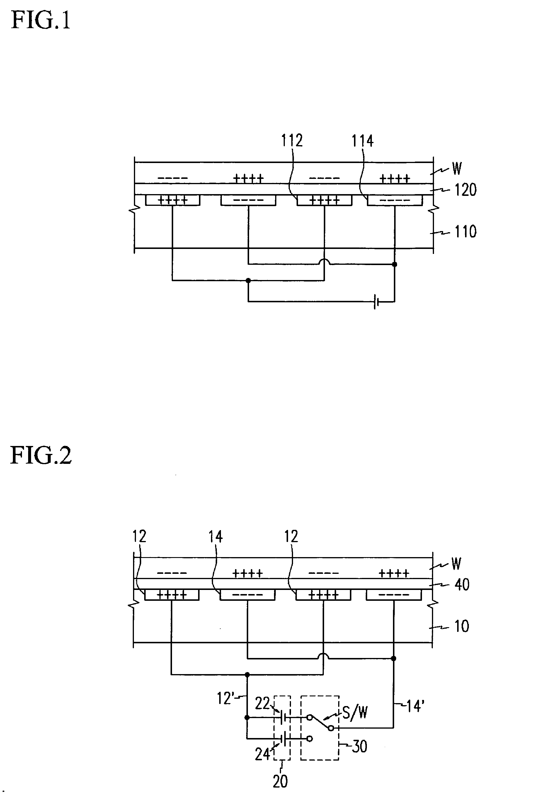
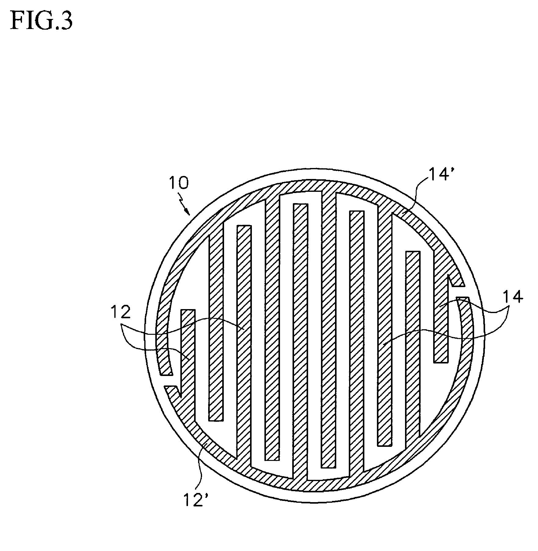
[0023]FIG. 2 and FIG. 3 are respectively a schematic view illustrating an electrostatic chuck and a top plan view of an electrode part of FIG. 2 according to a preferred embodiment of the present invention.

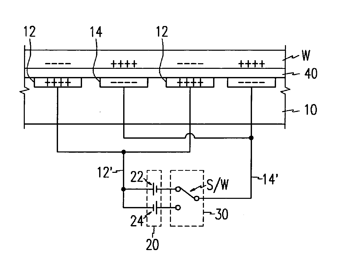
[0024] As shown in drawings, the electrostatic chuck according to the preferred embodiment of the present invention includes an electrode part 10, an electric source part 20, and a polarity inversion part 30.

[0025] The electrode part 10, which generates electric charge for fixing the wafer, includes first electrodes 12 and second electrodes 14 having different polarities. The first and second electrodes 12 and 14 are alternately arranged, and the electrodes having the same polarity are electrically conducted to by respective electric conductive parts 12 and 14′.

[0026] Here, the first electric conductive part 12 for conducting to the first electrodes 1...


PUM


Abstract

The present invention relates to an electrostatic chuck having electrodes of which polarities are periodically inverted, and a method for chucking wafers using the electrostatic chuck. The electrostatic chuck of the present invention includes an electrode part including first and second electrodes having different polarities and generating electrostatic charge for fixing a wafer, an electric source part having a first electric source for supplying positive and negative electricity to the respective first and second electrodes and a second electric source for supplying the negative and positive electricity to the respective first and second electrodes, and a polarity inversion part for inverting the polarities of the first and second electrodes every cycle.

Description

CLAIM OF PRIORITY [0001] This application makes reference to, incorporates the same herein, and claims all benefits accruing under 35 U.S.C. §119 from an application for ELECTROSTATIC CHUCK OF SEMICONDUCTOR FABRICATION EQUIPMENT AND METHOD FOR CHUCKING WAFER USING THE SAME filed in the Korean Industrial Property Office on Sep. 3, 2003 and there duly assigned Serial No. 10-2003-61554. BACKGROUND OF THE INVENTION [0002] (a) Field of the Invention [0003] The present invention relates to an electrostatic chuck of semiconductor fabrication equipment, and in particular, to a bipolar electrostatic chuck of which polarity is periodically alternated and a method for chucking wafers using the bipolar electrostatic chuck. [0004] (b) Description of the Related Art [0005] Typically, semiconductor devices are fabricated by repeatedly performing processes such as photolithography, etching, diffusion, ion implantation, metal deposition, chemical vapor deposition, etc. onto a wafer, and the wafers m...

Claims


Application Information

Patent Timeline
IPC IPC(8): H01L21/683H01L21/02H01T23/00
CPCH01L21/6833H01L21/02
Inventor KWON, YOUNG-MIN
Owner DONGBU ELECTRONICS CO LTD
Why Eureka
Try Eureka