
Semiconductor memory device

a memory device and semiconductor technology, applied in semiconductor devices, digital storage, instruments, etc., can solve the problems of difficult to obtain high-sensitivity, easy to flow a large cell current, and become impossible to perform high-speed read operation

Inactive Publication Date: 2005-03-03
KK TOSHIBA
View PDF7 Cites 146 Cited by
  • Summary
  • Abstract
  • Description
  • Claims
  • Application Information

AI Technical Summary

Benefits of technology

[0003] This invention relates to a semiconductor memory device of the type having a one-transistor / one-cell structure as formed on a silicon-on-insulator (SOI) substrate.

Problems solved by technology

Due to this, it is not easy to flow a large cell current, thereby resulting that it is not easy to obtain high-sensitivity.
If impossible to flow a large cell current, it takes a long time period for charging / discharging the bit line connected to a memory cell, whereby it becomes impossible to perform high-speed read operation.

Method used


Image

  • Semiconductor memory device
  • Semiconductor memory device
  • Semiconductor memory device

Examples


Embodiment Construction

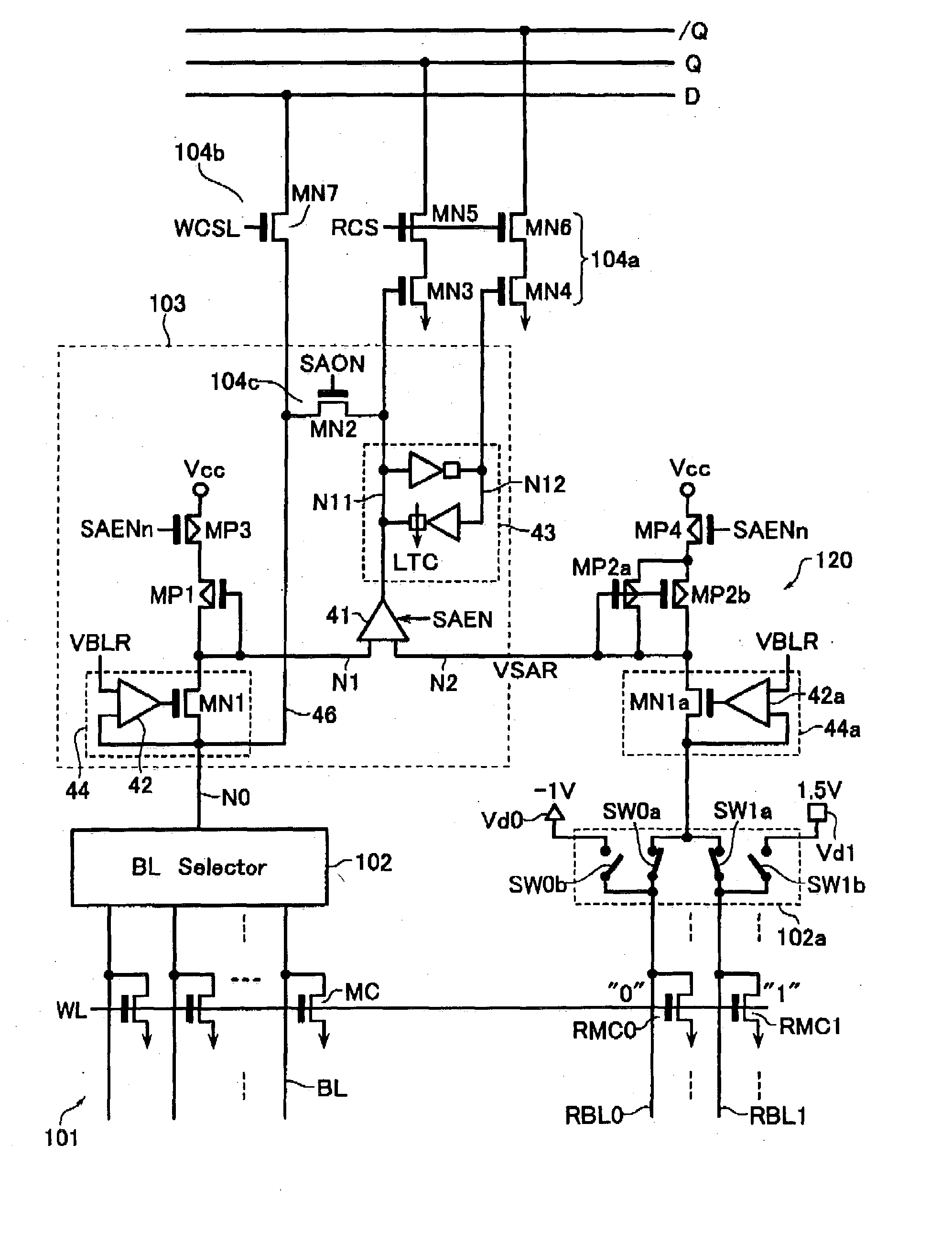
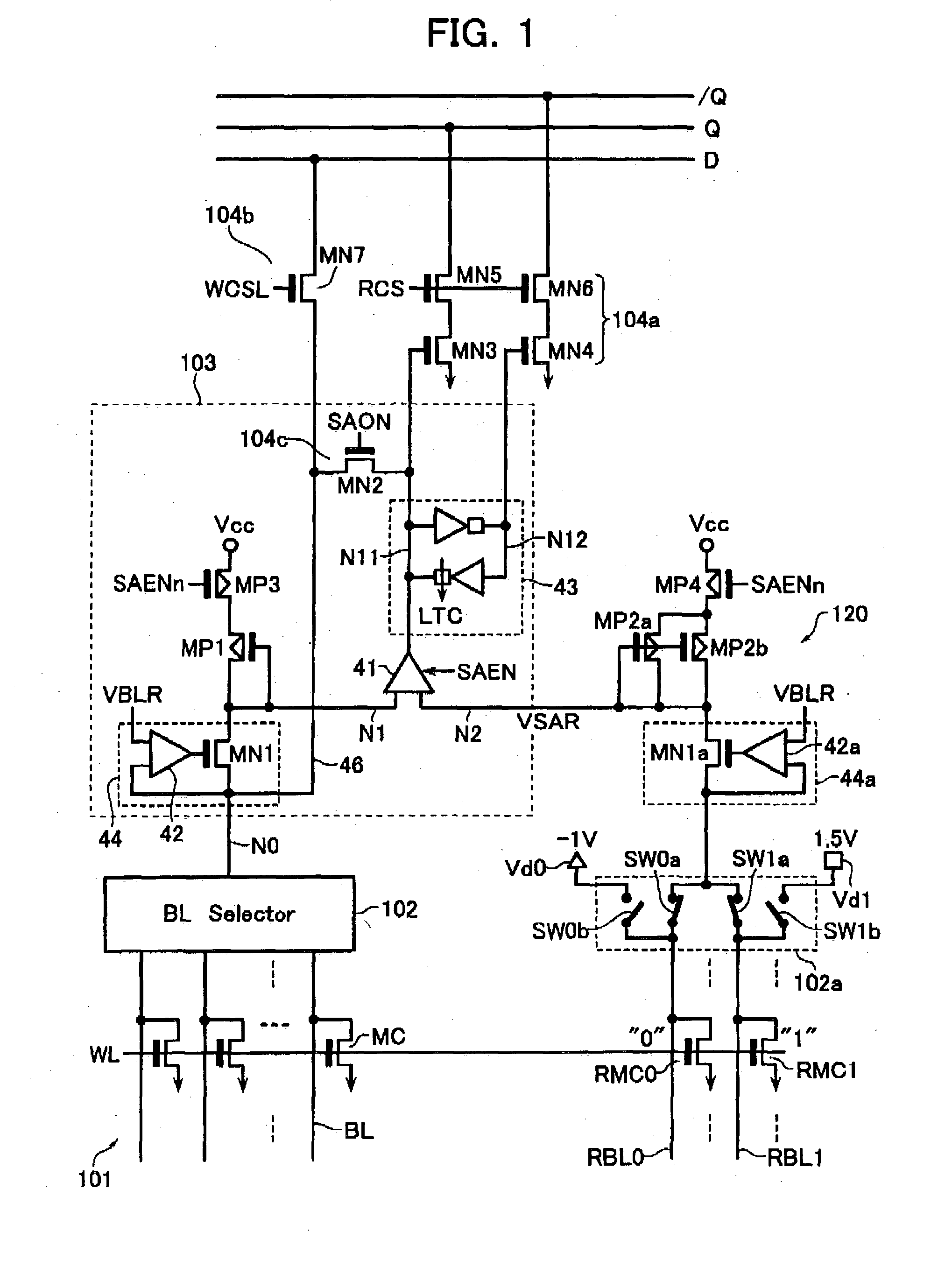
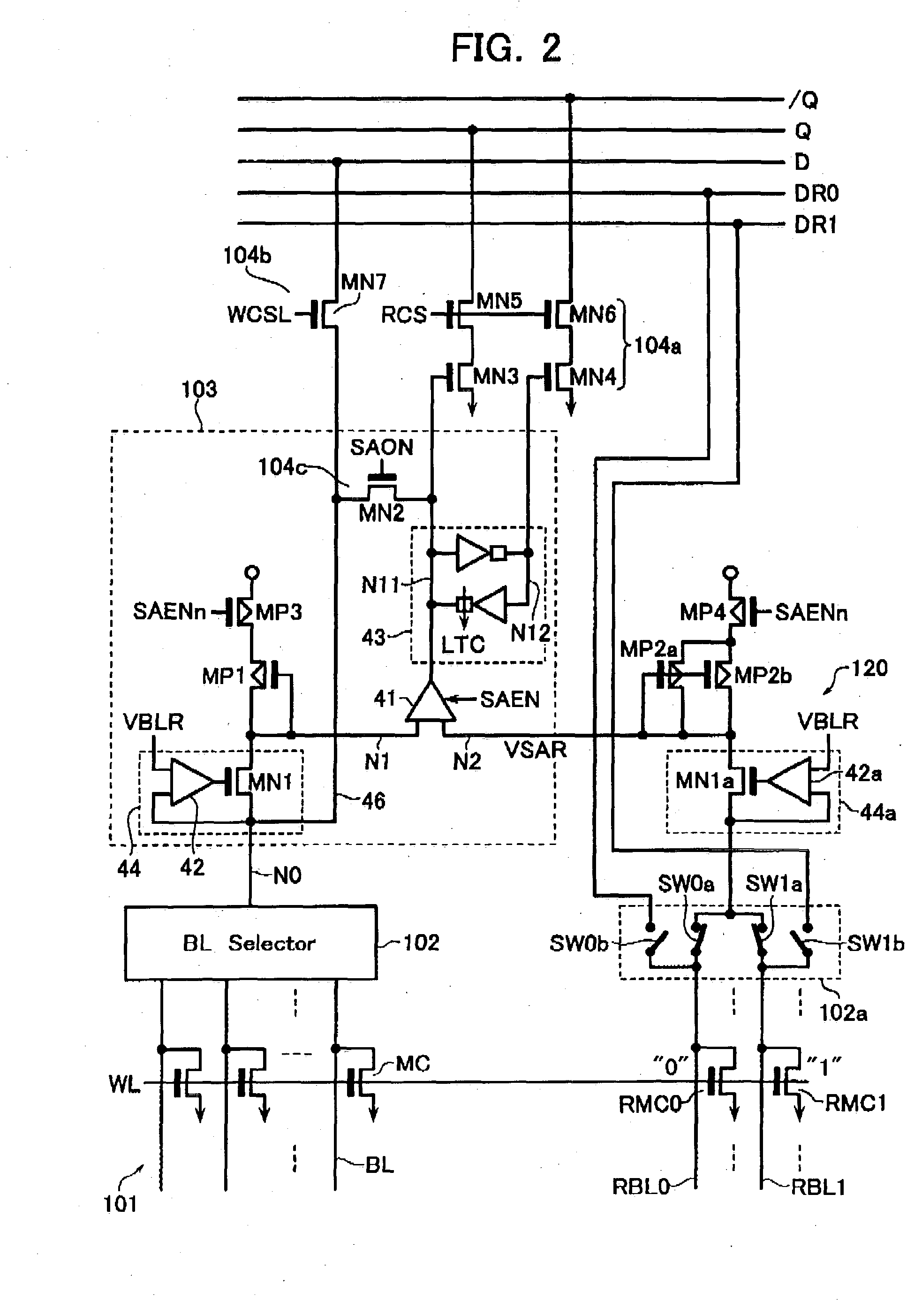
[0036] Illustrative embodiments of this invention will be explained with reference to the accompanying drawings below.

[0037] An explanation will first be given of the configuration of a memory cell array of a floating-body cell (FBC) memory device in accordance with one embodiment of the invention. FIG. 7 depicts a plan view of main part of the memory cell array, and FIGS. 8 to 10 are cross-sectional views of the cell array as taken along lines I-I′, II-II′ and III-III′, respectively.

[0038] The FBC memory has a silicon substrate 10 of P-type conductivity serving as a base substrate. The P-type substrate 10 has a top surface in which a heavily doped N (N+)-type layer 11 is formed with its surface covered or coated with an electrically insulative or dielectric film 12. This film may be a silicon oxide film or the like. On the dielectric film 12, a P-type silicon layer 13 is formed for use as an active layer which is electrically separated or isolated from substrate 10, thereby provi...


PUM


Abstract

A semiconductor memory device includes: a device substrate having a semiconductor layer separated by a dielectric layer from a base substrate; a memory cell array having a plurality of memory cells formed and arranged on the semiconductor layer of the device substrate, each the memory cell having a MOS transistor structure with a body in an electrically floating state to store data based on a majority carrier accumulation state of the body; and a sense amplifier circuit configured to read out data of a selected memory cell in the memory cell array to store the read data in a data latch, then transfer the read data to an output circuit and write back the read data into the selected memory cell.

Description

CROSS-REFERENCE TO RELATED APPLICATION [0001] This application is based on and claims the benefit of priority from the prior Japanese Patent Application No. 2003-132091, filed on May 9, 2003, the entire contents of which are incorporated herein by reference. BACKGROUND OF THE INVENTION [0002] 1. Field of the Invention [0003] This invention relates to a semiconductor memory device of the type having a one-transistor / one-cell structure as formed on a silicon-on-insulator (SOI) substrate. [0004] 2. Description of Related Art [0005] Recently, for the purpose of alternative use or replacement of conventional dynamic random access memory (DRAM) devices, a semiconductor memory device that has a more simplified cell structure for enabling achievement of dynamic storability has been proposed. This type of memory is disclosed, for example, in Takashi Ohsawa et al., “Memory Design Using One-Transistor Gain Cell on SOI”, ISSCC Digest of Technical Papers, 2002, pp. 152-153. [0006] A memory cell ...

Claims


Application Information

Patent Timeline
Patent Type & Authority Applications(United States)
IPC IPC(8): H01L27/108G11C7/06G11C11/401G11C11/404G11C11/406G11C11/4091G11C16/00H01L21/8242
CPCG11C7/062G11C7/067G11C11/406H01L29/7841G11C2207/065G11C2211/4016G11C2211/4068G11C11/4091G11C7/1051
Inventor IKEHASHI, TAMIOOHSAWA, TAKASHIFUJITA, KATSUYUKI
Owner KK TOSHIBA
Features
  • Generate Ideas
  • Intellectual Property
  • Life Sciences
  • Materials
  • Tech Scout
  • Unparalleled Data Quality
  • Higher Quality Content
  • 60% Fewer Hallucinations
Learn More