Method and apparatus for designing semiconductor integrated circuit

a technology of integrated circuits and semiconductors, applied in the direction of instruments, analogue processes for specific applications, electric/magnetic computing, etc., can solve the problems of increasing the design time, raising the design cost, and the provisional quantity and location of power supply pads cannot be accurately determined, so as to achieve accurate estimation of core size and core size

Inactive Publication Date: 2005-03-03
SOCIONEXT INC
View PDF12 Cites 30 Cited by
  • Summary
  • Abstract
  • Description
  • Claims
  • Application Information

AI Technical Summary

Benefits of technology

In the present invention, conditions of IR drop value and IO buffer current capacity that guarantee SI and PI can be satisfied when the circuit is laid out for the first time. As a result, redesigning of the layout of the circuit and a major correction, such as reselecting the LSI package or changing the chip size will not be necessary. In the present invention, when estimating t...

Problems solved by technology

The redesigning increases the design time and raises the design cost.
Thus, in the prior art...

Method used


Image

  • Method and apparatus for designing semiconductor integrated circuit
  • Method and apparatus for designing semiconductor integrated circuit
  • Method and apparatus for designing semiconductor integrated circuit

Examples


first embodiment

The first embodiment has the advantages described below.

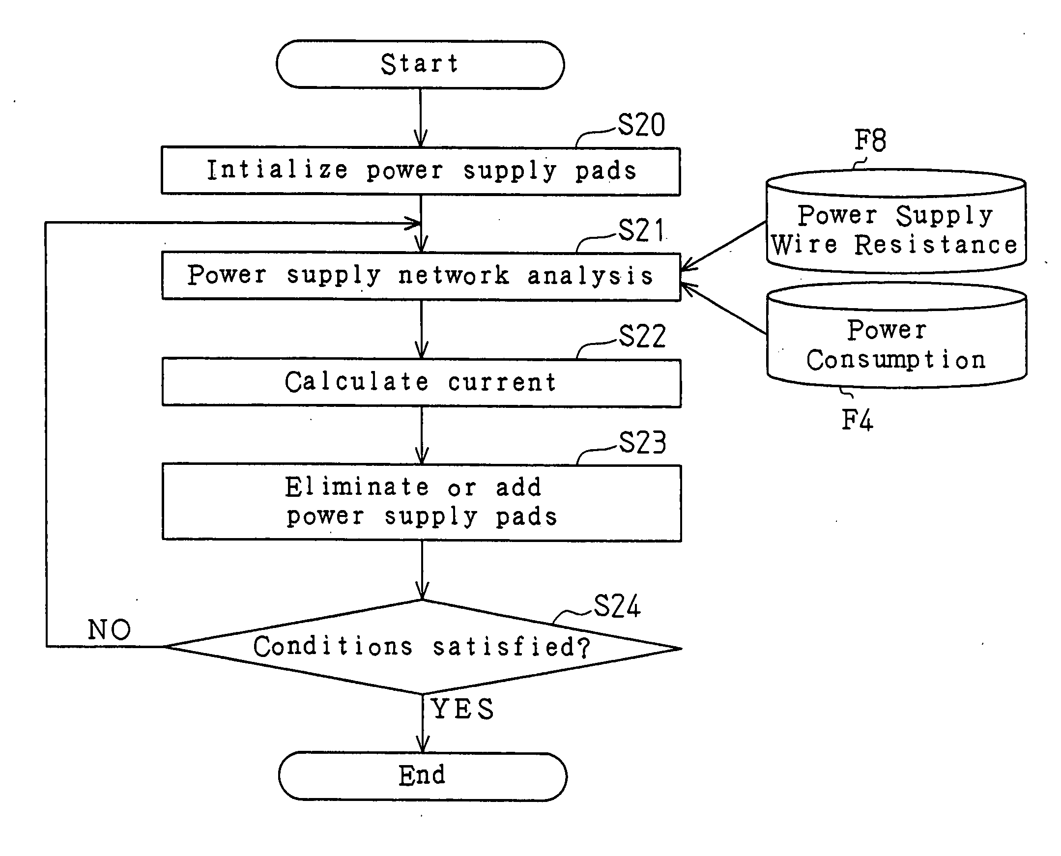
(1) The value of the current that flows through a power supply pad is calculated from the voltage value of each node that is obtained through the power supply network analysis. The current value and the current capacity of the IO buffer is then compared to determined the provisional quantity and provisional locations of the power supply pads. The provisional quantity and provisional locations of the power supply pads that guarantee the SI and PI taking into consideration the current capacity of the IO buffer are accurately estimated prior to the detailed layout. This decreases redesigning, shortens the design time, and reduces design costs.

(2) After the power supply network analysis, processing is suspended when the IR drop value between nodes exceeds the maximum IR drop value. Accordingly, the provisional quantity and the provisional locations of the power supply pads that satisfy the IR drop conditions in the core section ...

second embodiment

The second embodiment has the advantages described below.

(1) When the core section is configured by a plurality of circuit blocks, the core size is estimated as being the total area of the area of each circuit block, the wire region required when connecting circuit blocks, and the area of repeater cells that connect circuit blocks. This enables the minimum area of the core section, which is configured by a plurality of circuit blocks, to be accurately estimated.

It should be apparent to those skilled in the art that the present invention may be embodied in many other specific forms without departing from the spirit or scope of the invention. Particularly, it should be understood that the present invention may be embodied in the following forms.

In the procedure of the first embodiment that determines the provisional quantity and provisional locations of the power supply pads (FIG. 4), processing may be started in a state in which one power supply pad is provided for each side of ...


PUM


Abstract

A method for accurately determining the provisional quantity and provisional locations of power supply pads prior to detailed layout of a semiconductor integrated circuit. The method decreases redesigning, shortens the design time, and lowers design costs. The method includes performing a power supply network analysis of the core section to obtain voltage values of the nodes, calculating current values between the nodes from the voltage values of the nodes and the resistances between the nodes, and calculating current values of the power supply pads from the current values between the nodes. The method further includes determining whether to eliminate or add a power supply pad depending on whether the current value of each power supply pad exceeds the current capacity of an associated IO buffer.

Description

CROSS-REFERENCE TO RELATED APPLICATIONS This application is based upon and claims the benefit of priority from the prior Japanese Patent Application No. 2003-303495, filed on Aug. 27, 2003, the entire contents of which are incorporated herein by reference. BACKGROUND OF THE INVENTION The present invention relates to an apparatus and a method for efficiently designing a semiconductor integrated circuit. To produce a semiconductor integrated circuit (LSI), a floor plan is designed based on a netlist obtained through logic synthesizing. Cells are arranged and routed in accordance with the floor plan to layout the circuit in detail. The circuit undergoes simulation to determine whether the layout of the circuit guarantees signal integrity (SI) and power integrity (PI). The determination of whether the SI or the PI may be guaranteed is performed by determining whether or not an IR drop value (voltage drop value) exceeds a maximum value or by determining whether or not the value of th...

Claims


Application Information

Patent Timeline
IPC IPC(8): G06F9/45H01L21/82G06F17/50H01L21/822H01L27/04
CPCG06F17/5068G06F17/5036G06F30/367G06F30/39
Inventor KURIHARA, TAKASHITAKEUCHI, KAZUTAKA
Owner SOCIONEXT INC
Why Eureka
Try Eureka