Semiconductor device and manufacturing method thereof

a technology of semiconductor devices and manufacturing methods, applied in the direction of semiconductor devices, electrical devices, transistors, etc., can solve the problems of large size of parts connecting a plurality of fins, difficult to form the channel area b>7/b> having a width narrower than the gate length, and parasitic resistance becoming extremely larg

Inactive Publication Date: 2005-03-10
KK TOSHIBA
View PDF21 Cites 217 Cited by
  • Summary
  • Abstract
  • Description
  • Claims
  • Application Information

AI Technical Summary

Benefits of technology

[0034] According to an example of the present invention, there is provided a semiconductor device comprising: a semiconductor substrate; a fin-formed semiconductor layer which is formed on the semiconductor substrate, is long in a first direction and is short in a second direction crossing the first direction; a gate insulating layer formed on side surfaces of the semiconductor layer in the second direction; a gate electrode arranged so as to be adjacent to the gate insulating layer; a channel area formed at a posit...

Problems solved by technology

In each generation of LSI, however, since a dimension which can be processed into a minimum level by the lithography technology is usually coordinated with the gate length, it is very hard to form the channel area 7 having a width narrower than the gate length.
When a plurality of fins are connected to each other in parallel, however, a size of a part connecting a plurality of the fins is large.
As a result, in the tilted ion implantation method, impurities based on the ion implantation do not spread in the entire source/drain formation planned area in each fin, and there is a problem that an area which is of an electroconductive type opposite to that of the source/drain area partially remains in the source/drain formation planned area.
Additionally, when ...

Method used


Image

  • Semiconductor device and manufacturing method thereof
  • Semiconductor device and manufacturing method thereof
  • Semiconductor device and manufacturing method thereof

Examples


first embodiment

[0142] 2. First Embodiment

[0143] The first embodiment concerns a structure and a manufacturing method of a FinFET which realize suppression of the short channel effect, an increase in a drive current due to a reduction in a parasitic resistance, and others.

[0144] (1) Structure

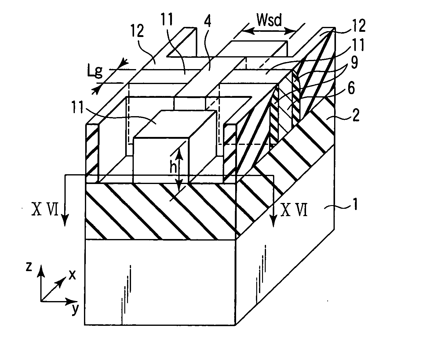
[0145]FIGS. 15 and 16 show a structure of the FinFET according to the first embodiment of the present invention. FIG. 16 is a cross-sectional view taken along the line XVI-XVI in FIG. 15.

[0146] An insulating layer 2 is formed on a silicon substrate 1, and a fin-shaped silicon layer 3 is formed on the insulating layer 2. A so-called SOI substrate is constituted by the silicon substrate 1, the insulating layer 2 and the silicon layer (fin) 3.

[0147] A cap insulating layer 4 used as a mask when processing the silicon layer 3 is formed on the insulating layer 2. A gate electrode 6 is formed on each of two side surfaces of the silicon layer 3 in a direction y through a gate insulating layer 5. Although the gate e...

second embodiment

[0194] 3. Second Embodiment

[0195] First, the second embodiment relates to a structure and a manufacturing method which facilitate formation of a fin and also facilitate subsequent processing of members using the photolithography or the like by controlling an effective channel width of the FinFET based on the number of fins connected to each other in parallel in place of heights of the fins.

[0196] Second, this embodiment relates to a structure and a manufacturing method which prevent an area which is of an electroconductive type different from an electroconductive type of a source / drain area from partially remaining in the source / drain area in the FinFET having such a structure that a plurality of fins are connected to each other in parallel.

[0197] (1) Structure

[0198]FIGS. 43 and 44 show a structure of a FinFET according to a second embodiment of the present invention. FIG. 44 is a cross-sectional view taken along the like XLIV-XLIV in FIG. 43.

[0199] An insulating layer 2 is form...

third embodiment

[0232] 4. Third Embodiment

[0233] The third embodiment relates to a structure and a manufacturing method by which a large part or all of a source / drain area is not silicided in a FinFET having a silicide layer on the source / drain area.

[0234] (1) Structure

[0235] Three examples will now be sequentially described hereinafter.

{circle over (1)} EXAMPLE 1

[0236]FIGS. 50 and 51 show a structural example 1 of a FinFET according to the third embodiment of the present invention. It is to be noted that FIG. 51 is a cross-sectional view taken along the line LI-LI in FIG. 50.

[0237] An insulating layer 2 is formed on a silicon substrate 1, and a fin-shaped silicon layer 3 which is long in a direction x and short in a direction y is formed on the insulating layer 2. A so-called SOI substrate is constituted by the silicon substrate 1, the insulating layer 2 and the silicon layer (fin) 3.

[0238] Gate electrodes 6 are formed on two side surfaces of the silicon layer 3 in a direction Y through gate...


PUM


Abstract

A semiconductor layer in which a primary part of a FinFET is formed, i.e., a fin has a shape which is long in a direction x and short in a direction y. A width of the fin in the direction y changes on three stages. First, in a channel area between gate electrodes each having a gate length Lg, the width of the fin in the direction y is Wch. Further, the width of the fin in the direction y in a source/drain extension area adjacent to the channel area in the direction x is Wext (>Wch). Furthermore, the width of the fin in the direction y in a source/drain area adjacent to the source/drain extension area in the direction x is Wsd (>Wext).

Description

CROSS-REFERENCE TO RELATED APPLICATIONS [0001] This application is based upon and claims the benefit of priority from prior Japanese Patent Application No. 2003-317259, filed Sep. 9, 2003, the entire contents of which are incorporated herein by reference. BACKGROUND OF THE INVENTION [0002] 1. Field of the Invention [0003] The present invention relates to a semiconductor device having an MIS type field effect transistor and a manufacturing method thereof. [0004] 2. Description of the Related Art [0005] In recent years, as demands for a realization of a semiconductor integrated circuit with low power consumption and high operating speed or the like become rigid, a realization of a low power supply voltage and a fine element is desired. For this reason, in regard to a transistor element, attention is paid to a three-dimensional element in place of a conventional planar type element. [0006] As the three-dimensional element, there has been known, e.g., an MOS transistor utilizing a fin-s...

Claims


Application Information

Patent Timeline
IPC IPC(8): H01L21/336H01L29/417H01L29/45H01L29/786
CPCH01L21/26586H01L29/41733H01L29/458H01L29/785H01L29/66803H01L29/66818H01L29/66545
Inventor FUJIWARA, MAKOTOISHIMARU, KAZUNARIHOKAZONO, AKIRA
Owner KK TOSHIBA
Why Eureka
Try Eureka