Sense amplifier power-gating technique for integrated circuit memory devices and those devices incorporating embedded dynamic random access memory (DRAM)

a technology of integrated circuit memory and dynamic random access memory, which is applied in the direction of information storage, static storage, digital storage, etc., can solve the problems of concomitant slow “read”, “write” speed, and tend to latch very late, so as to minimize the on-chip area requirements and ensure the effect of speed

Inactive Publication Date: 2005-03-10
SONY CORP
View PDF14 Cites 9 Cited by
  • Summary
  • Abstract
  • Description
  • Claims
  • Application Information

AI Technical Summary

Benefits of technology

[0009] In accordance with the present invention, a sense amplifier power-gating circuit and method is disclosed which is of particular utility with respect to DRAM devices, or those incorporating embedded DRAM, having a power-down (or Sleep) mode of operation. In accordance with the technique of the present invention, the local sense amplifier driver transistors also serve a dual purpose as power gate transistors. In an Active Mode (during sensing), there transistors are turned “on” (LPB=VSS, LNB=VCC) and turned “off” (LPB=VCC, LNB=VSS) when the sense amplifier array is deactivated (during bit line precharge operations, or Standby Mode). During a Sleep Mode, a negative VGS is applied to these transistors to reduce the current through the sense amplifiers through LPB being driven to a voltage above VCC while LNB is driven to a voltage below VSS (e.g. LPB=VCC+0.3V, LNB=VSS−0.3V). Through implementation of the technique of the present invention, large, distinct power gate transistors are not required, thereby minimizing on-chip area requirements, and sensing speed is not degraded as with conventional approaches.

Problems solved by technology

Because of this, relatively slow latching speeds may be experienced resulting in concomitantly slow “read” and “write” speeds.
Moreover, data patterns may be encountered which can cause failures such as a logic level “1” in a field of “0s” will tend to latch very late if the number of sense amplifiers in the column is large.
However, since there would typically be a large number of sense amplifiers coupled to these power gate transistors, and all of these sense amplifiers would be switching at about the same time, the current surge through the power gate transistors during a sensing operation ends up being very large.
This current surge causes a voltage drop across the power gate transistors which tends to have the same effect as reducing the level of VCC, thereby degrading sensing speed.
Furthermore, these sense amplifier power gate transistors must, of necessity, be made extremely large to avoid degrading circuit speed too much, (although such degradation nonetheless occurs to at least some extent) thereby consuming a great deal of on-chip area.

Method used


Image

  • Sense amplifier power-gating technique for integrated circuit memory devices and those devices incorporating embedded dynamic random access memory (DRAM)
  • Sense amplifier power-gating technique for integrated circuit memory devices and those devices incorporating embedded dynamic random access memory (DRAM)
  • Sense amplifier power-gating technique for integrated circuit memory devices and those devices incorporating embedded dynamic random access memory (DRAM)

Examples


Embodiment Construction

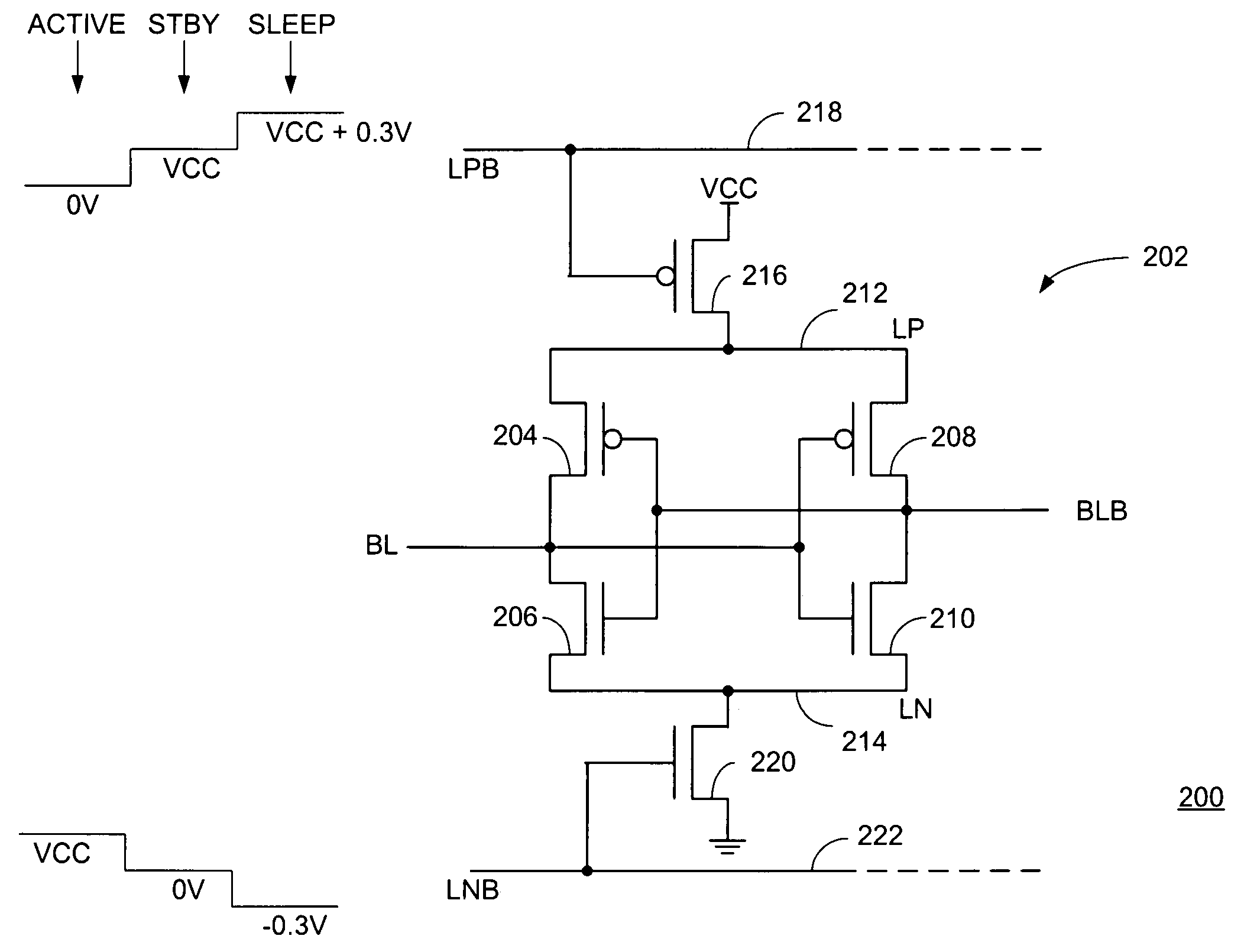
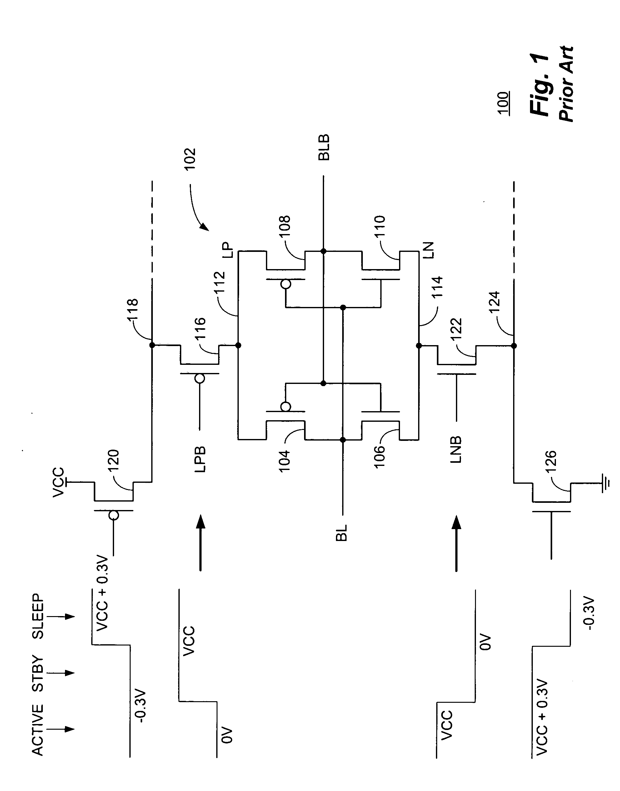
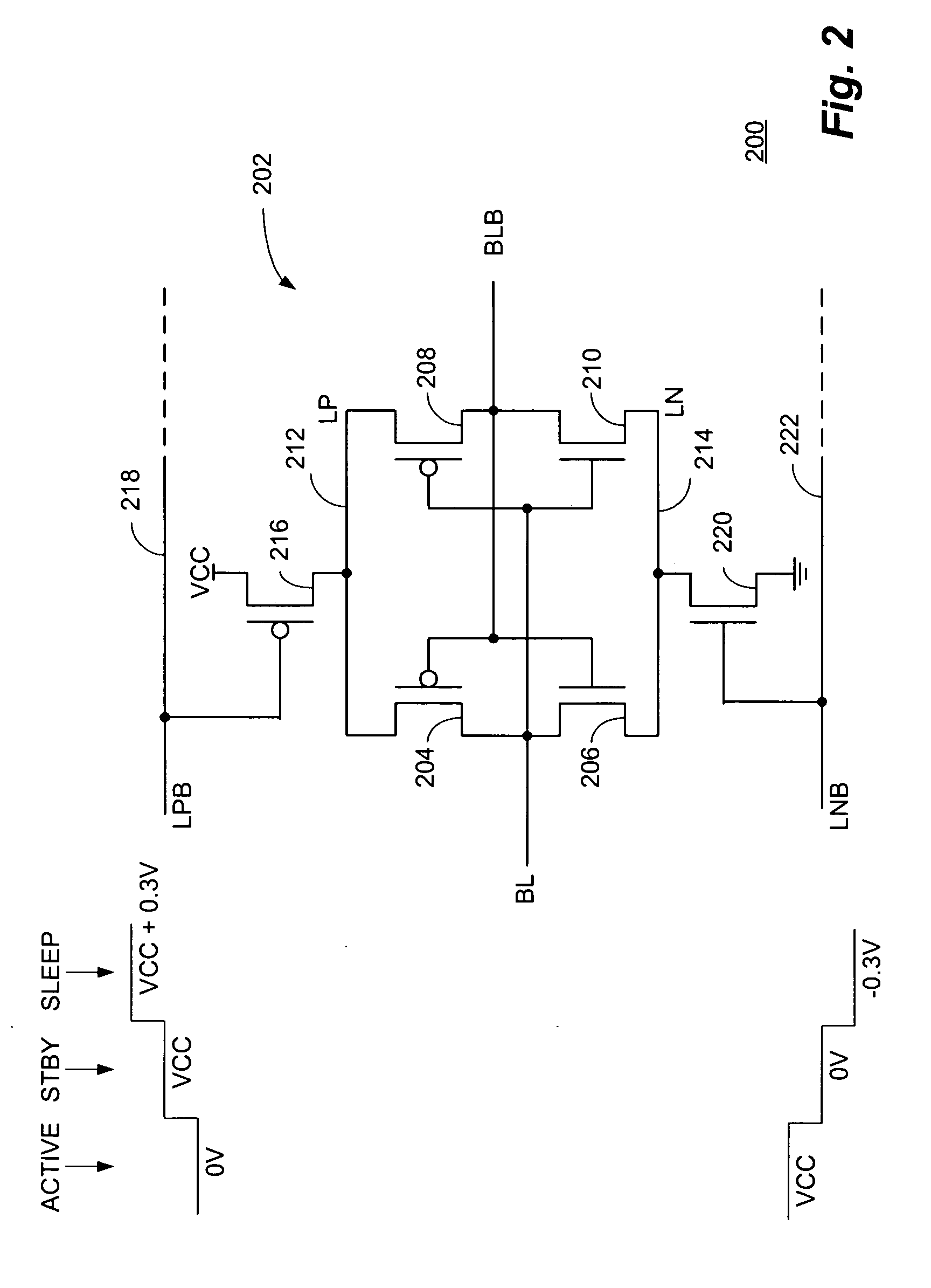
[0020] With reference now to FIG. 1, a schematic illustration of a conventional sense amplifier circuit 100 for a DRAM array is shown incorporating a conventional power-gating technique. The conventional sense amplifier circuit 100 comprises, in pertinent part, a sense amplifier 102 in the form of a latch comprising a pair of cross-coupled CMOS inverters.

[0021] A P-channel transistor 104 is connected in series with an N-channel transistor 106, with their gate terminals connected together and their drain terminals coupled to a bit line (BL). Another P-channel transistor 108 is connected in series with an N-channel transistor 110 with their gate terminals connected together to the bit line (BL) and their drain terminals connected to a complementary bit line (BLB) and the gate terminals of transistors of transistors 104, 106. The source terminals of transistors 104 and 108 are connected to an LP (latch P-channel) node 112 while the source terminals of transistors 106 and 110 are conne...


PUM


Abstract

A sense amplifier power-gating circuit and method is disclosed which is of particular utility with respect to DRAM devices, or those incorporating embedded DRAM, and having a power-down (or Sleep) mode of operation. In accordance with a particular technique of the present invention, the local sense amplifier driver transistors serve a dual purpose as both driver and power gate transistors thereby obviating the need for large, distinct power-gating devices. This serves to minimize on-chip area requirements while not degrading sensing speed as in conventional approaches.

Description

CROSS REFERENCE TO RELATED PATENT APPLICATIONS [0001] The present invention is related to, and claims priority from, U.S. Provisional Patent Application Ser. No. 60 / 500,126 filed Sep. 4, 2003 for: “0.6V 205 MHz 19.5 nsec TRC 16 Mb Embedded DRAM” the disclosure of which is herein specifically incorporated in its entirety by this reference. The present invention is further related to the subject matter disclosed in U.S. patent applications Ser. No. [UMI-359] entitled “Column Read Amplifier Power-Gating Technique for Integrated Circuit Memory Devices and Those Devices Incorporating Embedded Dynamic Random Access Memory (DRAM)⇄ and [UMI-360] entitled: “High Speed Power-Gating Technique for Integrated Circuit Devices Incorporating a Sleep Mode of Operation”, the disclosures of which are herein specifically incorporated by this reference in its entirety.BACKGROUND OF THE INVENTION [0002] The present invention relates, in general, to the field of integrated circuit memory devices and those...

Claims


Application Information

Patent Timeline
Patent Type & Authority Applications(United States)
IPC IPC(8): G11C7/00G11C11/409G11C7/06
CPCG11C7/065G11C2207/2227G11C2207/065
Inventor HARDEE, KIM C.
Owner SONY CORP
Why Eureka
Try Eureka