

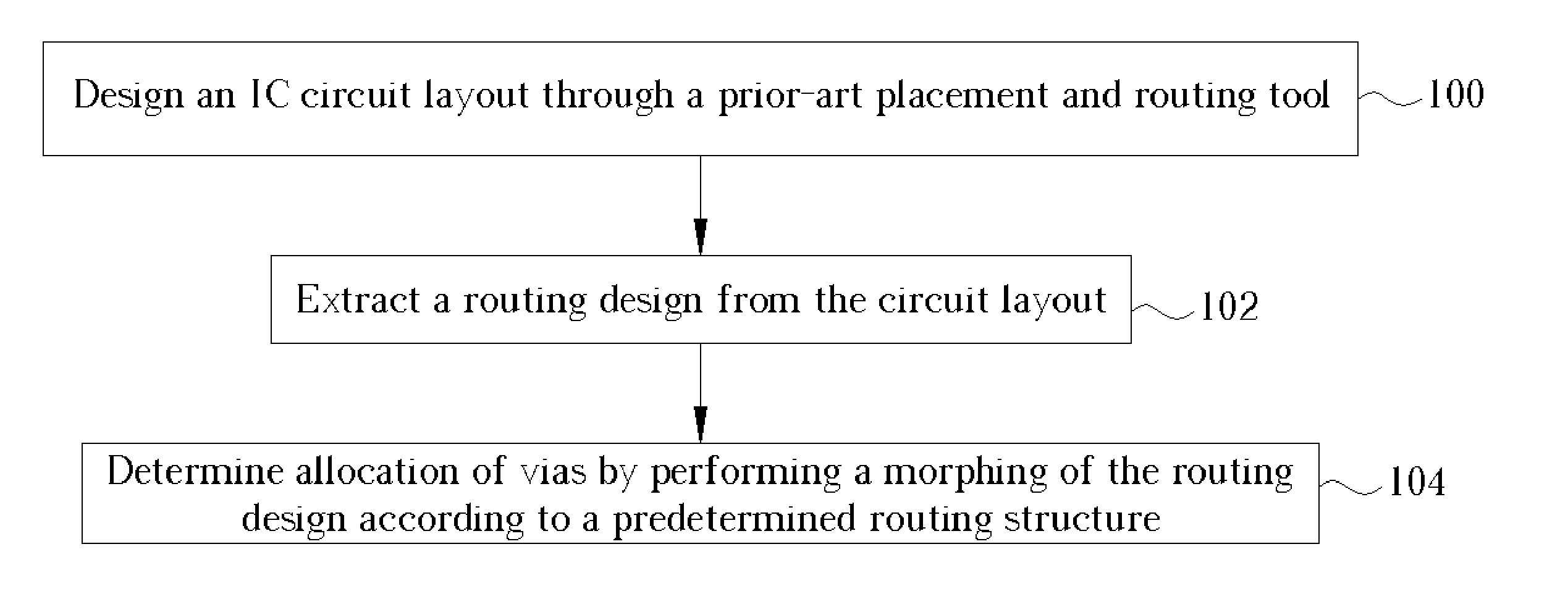
Method for programming a routing layout design through one via layer
a routing layout and routing layout technology, applied in the direction of conductive pattern formation, semiconductor/solid-state device details, instruments, etc., can solve the problems of increasing the cost of photomasks will occupy a great proportion of the total fabrication cost of ic, etc., and achieve the effect of avoiding the addition of the cost of various photomasks for different ics
- Summary
- Abstract
- Description
- Claims
- Application Information
AI Technical Summary
Benefits of technology
Problems solved by technology
Method used
Image

Examples
Embodiment Construction
[0021]FIG. 3 is a schematic diagram of the routing layout applied to a one metal programmable cell array (OMPCA) 50 according to the present invention. As shown in FIG. 3, a semiconductor body 52 comprises a plurality of basic units 54 thereon, wherein the basic units 54 are arranged as an array. Each basic unit 54 comprises at least a look-up table cell 56, a driving cell 58, and a storage element 60. The basic units 54 are prefabricated on the semiconductor body 52 in a wafer factory. Then, an IC designer can program the routing layout of the metal layers on the semiconductor body 52 according to the function and requirement of the IC so as to design the functionality of each of the look-up table cells 56, driving cells 58, and storage elements 60 of each basic units 54 and the connections among the basic units 54. Afterward, the wafer factory forms the metal layers on the semiconductor body 52 by several photomasks according to the design of the routing layout so as to accomplish...
PUM
| Property | Measurement | Unit |
|---|---|---|
| lengths | aaaaa | aaaaa |
| capacitances | aaaaa | aaaaa |
| resistances | aaaaa | aaaaa |
Abstract
Description
Claims
Application Information