Light emission device and manufacturing method thereof

Inactive Publication Date: 2005-03-17
FUJIFILM HLDG CORP
View PDF0 Cites 39 Cited by
  • Summary
  • Abstract
  • Description
  • Claims
  • Application Information

AI Technical Summary

Benefits of technology

[0013] This configuration ensures superior heat radiation properties without the need for any expensive fine-processing techniques,

Problems solved by technology

But because glass epoxy is inferior in heat radiation properties, where the light emitting elements are to be mounted highly densely, a metallic material, such as aluminum or metal core, or ceramics are used as the substrate material.
However, in comparison with the general cases where the circuit

Method used


Image

  • Light emission device and manufacturing method thereof
  • Light emission device and manufacturing method thereof
  • Light emission device and manufacturing method thereof

Examples


Embodiment Construction

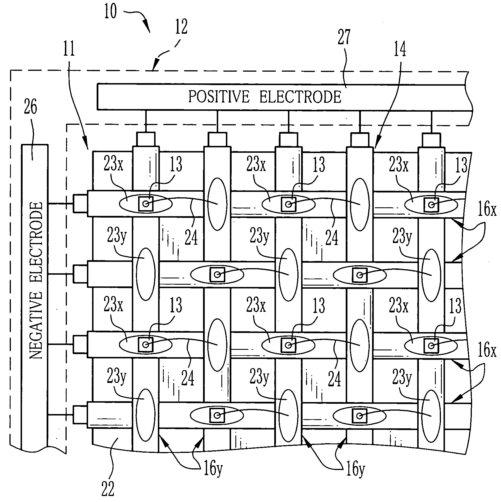
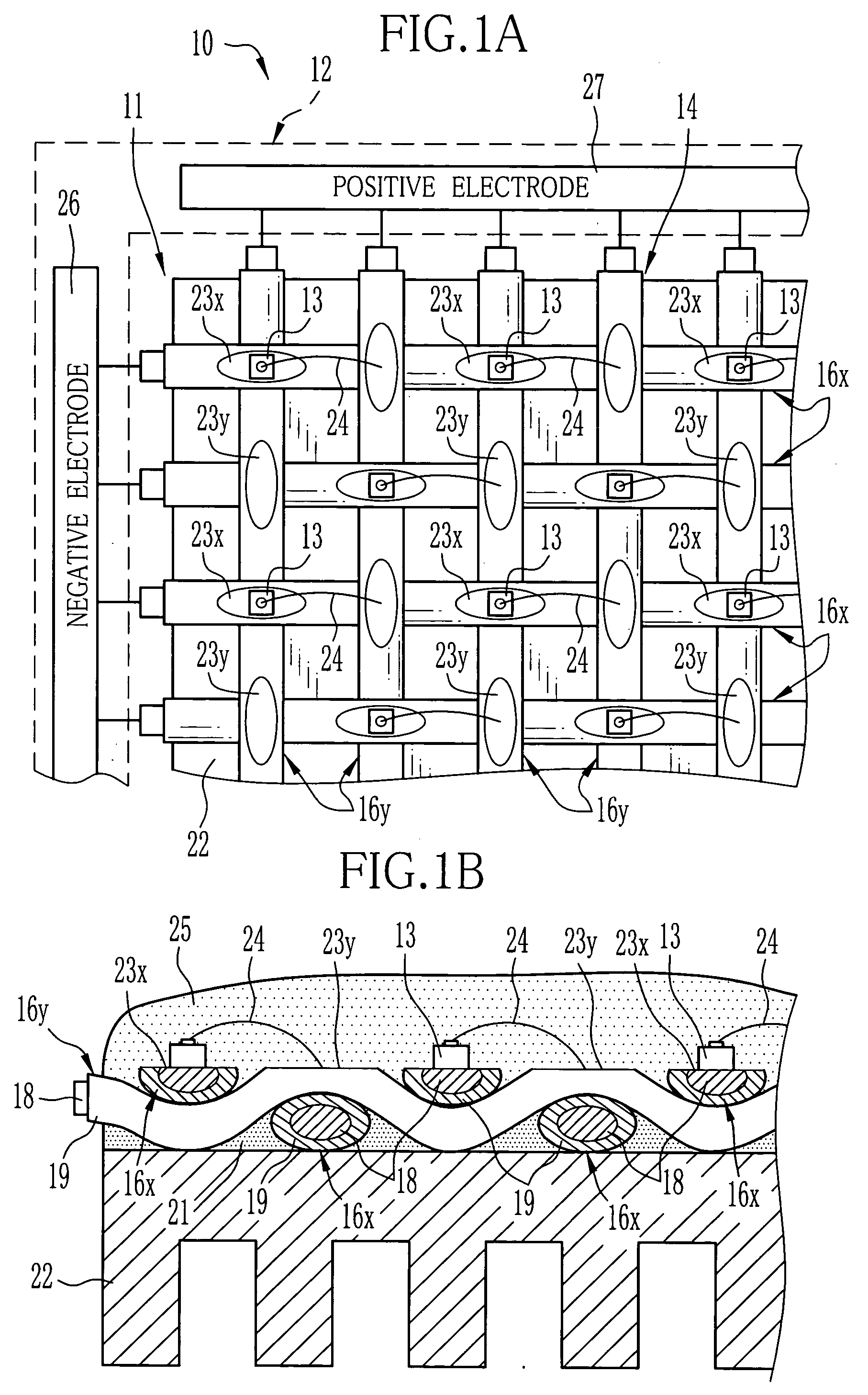
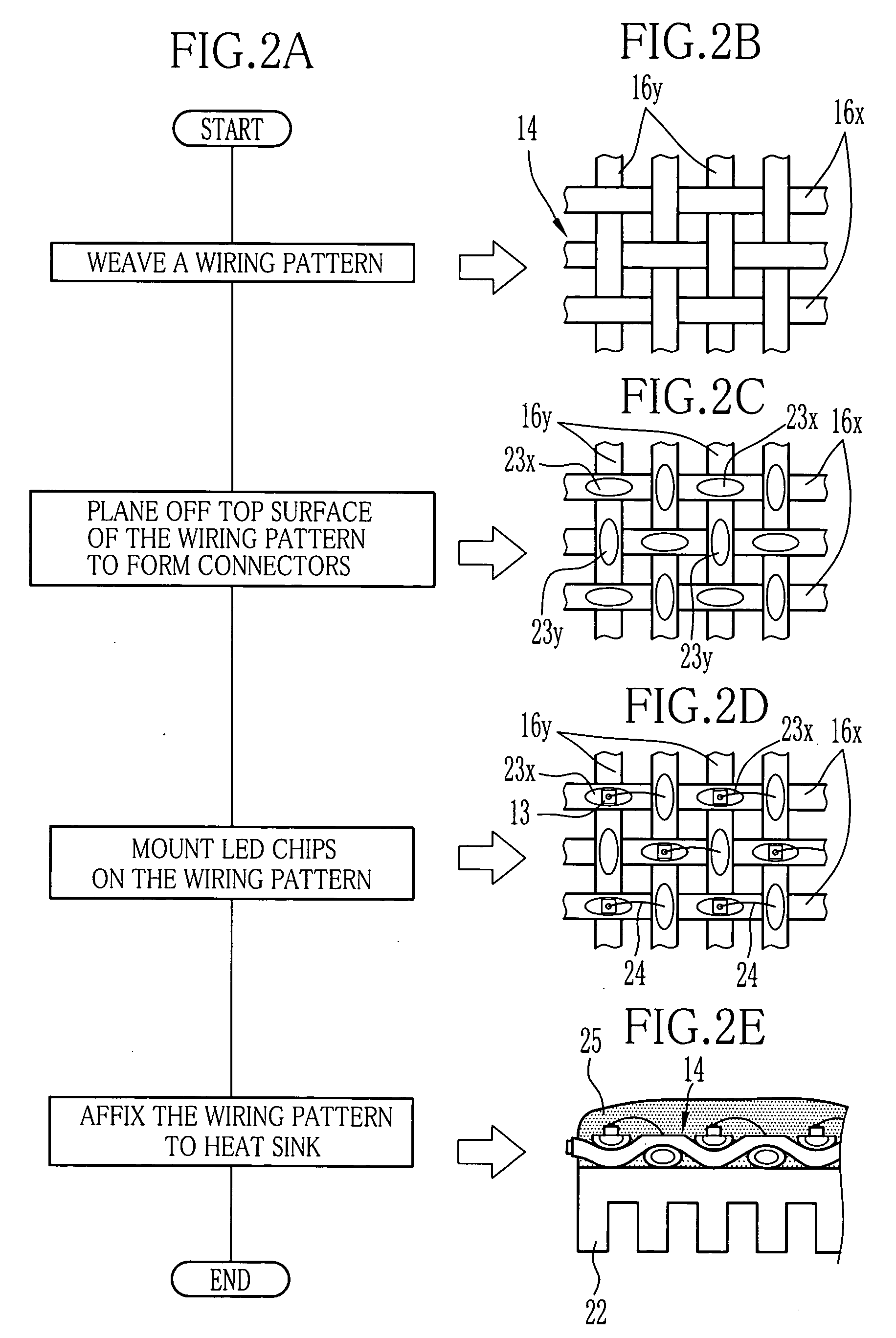
[0022] As shown in FIG. 1A, a light emission device 10 consists of a main body 11 and a driver circuit 12. The main body 11 has a large number of LED (light emitting diode) chips 13 as light emitting elements, and a wiring pattern 14 that connects the respective LED chips 13 to the driver circuit 12. The LED chips 13 are arranged in a matrix, and are mounted on the wiring pattern 14. The driver circuit 12 applies a voltage on the LED chips 13 to turn them on.

[0023] The wiring pattern 14 is produced by weaving a number of lateral line members 16x and a number of longitudinal line members 16y into a cross grid, as shown in FIGS. 1A and 1B. The lateral direction and the longitudinal direction of the wiring pattern 14 may be called X-direction and Y-direction respectively. Each line member 16x or 16y is made by coating an electro conductive core 18 with an isolating material 19. The lateral line members 16x are isolated from the longitudinal line members 16y, and provide minus or negat...


PUM


Abstract

A light emission device is constituted of LED chips, a driver circuit, and a wiring pattern for connecting the individual LED chips to the driver circuit. The wiring pattern is formed by weaving line members into a cross grid, the line member being formed by coating an electro conductive core with an isolating material. The lateral line members are connected to a negative electrode of the driver circuit, while the longitudinal line members are connected to a positive electrode of the driver circuit. Connectors are formed at cross points between the line members Negative poles of the LED chips are connected to the connectors that are formed on the lateral line members, while positive poles of the LED chips are connected to the connectors that are formed on the longitudinal line members. The wiring pattern is affixed to a heat sink through an adhesive agent.

Description

FIELD OF THE INVENTION [0001] The present invention relates to a light emission device having a number of light emitting elements arranged in a pattern, and also to a manufacturing method of the light emission device. BACKGROUND ARTS [0002] There have been known light emission devices having a number of light emitting elements, such as light emission diodes, arranged in a matrix, for example, in Japanese Laid-open Patent Applications Nos. Hei 7-287535 and 6-301342. These light emission devices are used as illuminations, optical fixing devices, or display panels. For use as a display panel, the light emitting elements are individually controlled on and off. The light emitting elements are mounted on an implemental surface of a substrate, where a circuit pattern is formed to connect the light emitting elements electrically to a driver circuit. [0003] As well-known in the art, the circuit pattern is formed on the substrate, which has a number of electro conductive layers and isolating ...

Claims


Application Information

Patent Timeline
IPC IPC(8): G09F9/30G09F9/00G09F9/33H01L25/075H01L33/56H01L33/62H01L33/64
CPCH01L25/0753H01L33/62H01L24/32H01L2224/73265H01L2224/48091H01L2924/00014H01L2924/00H01L2924/12042H01L2924/12041H01L2924/181H01L2924/00012G09F9/33
Inventor MIZUYOSHI, AKIRA
Owner FUJIFILM HLDG CORP
Why Eureka
Try Eureka