Methods for identifying non-volatile memory elements with poor subthreshold slope or weak transconductance

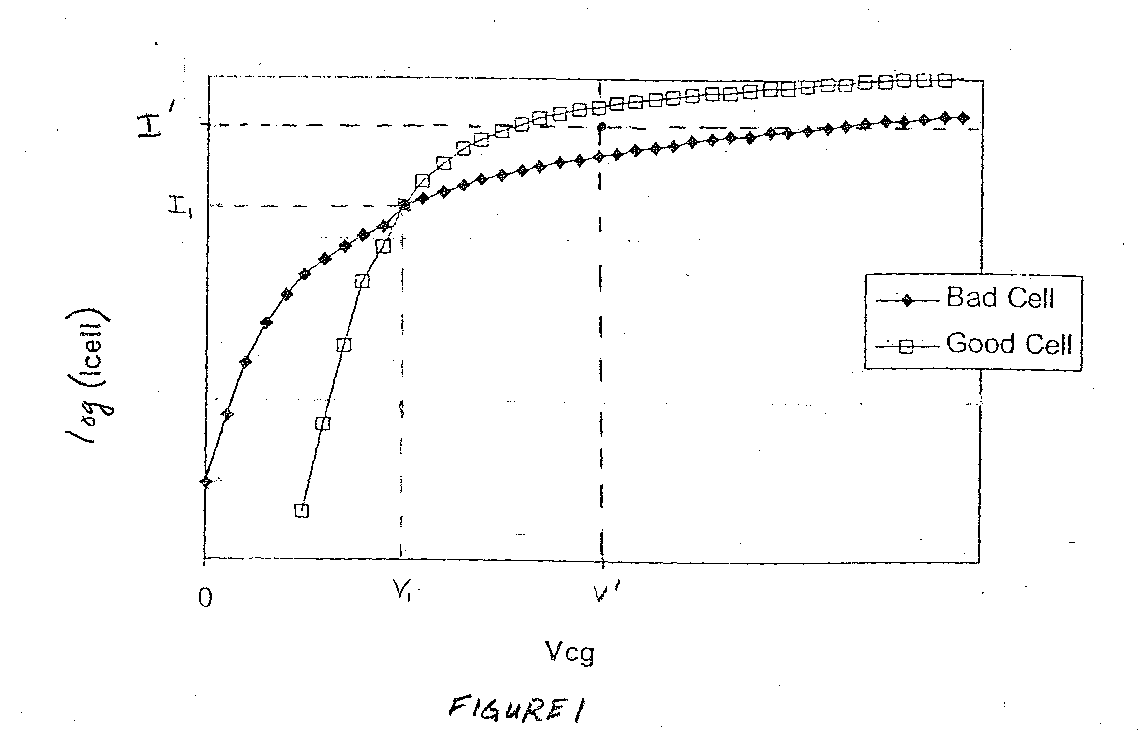
a non-volatile memory and subthreshold slope technology, applied in the field of non-volatile memories, can solve the problems of small widow of available threshold voltage, weak transconductance, flash memory cells are known to suffer from poor subthreshold slope or weak transconductance, etc., to achieve the effect of increasing the effect, reducing the transconductance, and poor subthreshold slop

Active Publication Date: 2005-03-17
SANDISK TECH LLC +1
View PDF11 Cites 24 Cited by
  • Summary
  • Abstract
  • Description
  • Claims
  • Application Information

AI Technical Summary

Problems solved by technology

The trend towards lower power systems results in a smaller widow of available threshold voltages, further aggravating this problem.
Occasionally, flash memory cells are known to suffer from poor subthreshold slope or weak transconductance.
The cells have a reduced conductivity, but more importantly their turn-off characteristics, defined by their subthreshold slope, are very poor.
These cells can cause stored data to be corrupted if the subthreshold slope deteriorates to the point that the cell is still conducting even when the gate voltage is below the cell threshold.
This significantly reduces the read margin and makes the cell very susceptible to “flipping bits” if the read conditions are varied.
Additionally, it has been found that bad cells tend to drift form their programmed value at a faster rate than the good cells.

Method used


Image

  • Methods for identifying non-volatile memory elements with poor subthreshold slope or weak transconductance
  • Methods for identifying non-volatile memory elements with poor subthreshold slope or weak transconductance
  • Methods for identifying non-volatile memory elements with poor subthreshold slope or weak transconductance

Examples


Embodiment Construction

[0022] Example Non-Volatile Memory System

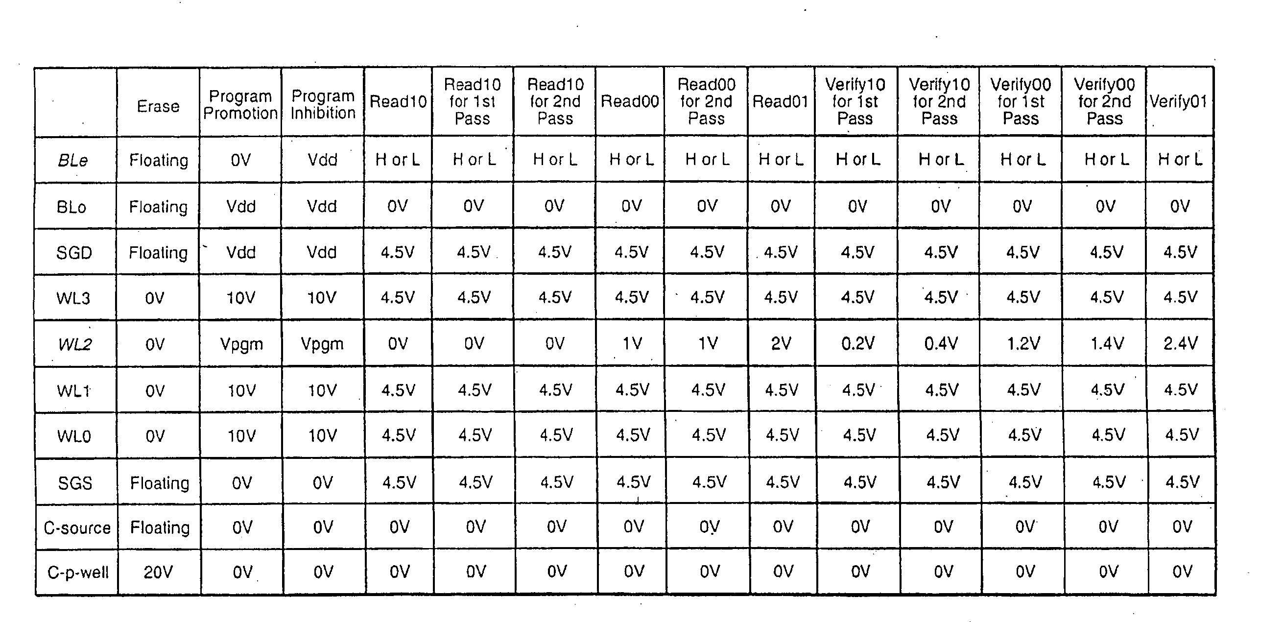
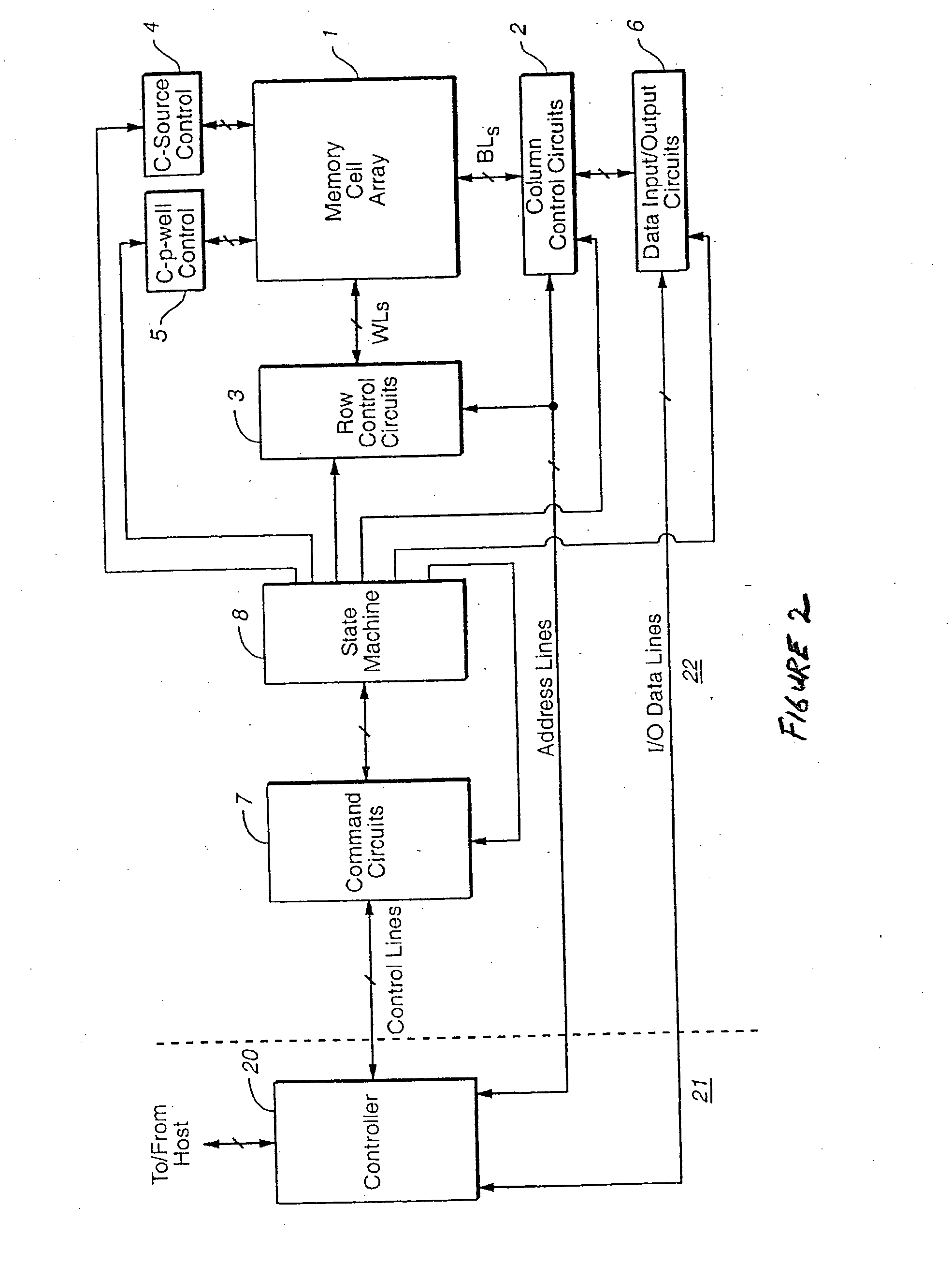
[0023] With reference to FIGS. 2-5, an exemplary non-volatile memory system is described in which the various aspects of the present invention are implemented, in order to provide specific examples. (FIGS. 2-5 are adapted from U.S. Pat. No. 6,456,528, which is hereby incorporated by reference, and are described there in further detail.) FIG. 2 is a block diagram of a flash memory system. Memory cell array 1 includes a plurality of memory cells M arranged in a matrix is controlled by a column control circuit 2, a row control circuit 3, a c-source control circuit 4 and a c-p-well control circuit 5. The column control circuit 2 is connected to bit lines (BL) of the memory cell array 1 for reading data stored in the memory cells (M), for determining a state of the memory cells (M) during a program operation, and for controlling potential levels of the bit lines (BL) to promote the programming or to inhibit the programming. The row control circui...


PUM


Abstract

The present invention presents a number of methods for identifying cells with poor subthreshold slope and reduced transconductance. A first set of techniques focuses on the poor subthreshold behavior of degraded storage elements by cycling cells and then programming them to a state above the ground state and the reading them with a control gate voltage below the threshold voltage of this state to see if they still conduct. A second set of embodiments focuses on weak transconductance behavior by reading programmed cells with a control gate voltage well above the threshold voltage. A third set of embodiments alters the voltage levels at the source-drain regions of the storage elements. The current-voltage curve of a good storage element is relatively stable under this shift in bias conditions, while degraded elements exhibit a larger shift. The amount of shift can be used to differentiate the good elements from the bad.

Description

FIELD OF THE INVENTION [0001] This invention relates generally to non-volatile memories and its operation, and, more specifically, to the determination of defective storage elements of the memory. BACKGROUND OF THE INVENTION [0002] The principles of the present invention have application to various types of non-volatile memories, those currently existing and those contemplated to use new technology being developed. Implementations of the present invention, however, are described with respect to a flash electrically erasable and programmable read-only memory (EEPROM), wherein the storage elements are floating gates, as exemplary. [0003] It is common in current commercial products for each floating gate storage element of a flash EEPROM array to store a single bit of data by operating in a binary mode, where two ranges of threshold levels of the floating gate transistors are defined as storage levels. The threshold levels of a floating gate transistor correspond to ranges of charge le...

Claims


Application Information

Patent Timeline
Patent Type & Authority Applications(United States)
IPC IPC(8): G01R31/28G11C16/02G11C16/04G11C16/34G11C29/50G11C29/56H01L21/8247H01L27/115H01L29/788H01L29/792
CPCG11C16/04G11C16/349G11C29/50004G11C29/50G11C16/3495G11C16/34G11C16/10
Inventor LUTZE, JEFFREY W.CHEN, JIANLI, YANKANEBAKO, KAZUNORITANAKA, TOMOHARU
Owner SANDISK TECH LLC
Why Eureka
Try Eureka