Semiconductor device

a technology of semiconductor devices and memory cells, applied in the direction of information storage, static storage, digital storage, etc., can solve the problems of disadvantageous data storage and inability to perform a refresh operation for memory cells during this period, and achieve the effect of shortening the time necessary for this write operation and performing in a short tim

Active Publication Date: 2005-03-17
CETUS TECH INC
View PDF6 Cites 10 Cited by
  • Summary
  • Abstract
  • Description
  • Claims
  • Application Information

AI Technical Summary

Benefits of technology

[0036] Moreover, according to an embodiment, after writing externally supplied input data in main amplifiers selected in response to a column address, the input data of these main amplifiers can be written in memory cells selected in response to a row address. Therefore, in repeatedly writing specific data in a given region of a memory cell array, data can be written in memory cells by regarding, as a unit, a group of main amplifiers selected in response to the column address, and time necessary for this write operation can be shortened.
[0037] In addition, according to an embodiment, after writing data of a plurality of memory cells selected in response to a row address in the main amplifiers through the sense amplifiers, the data of these main amplifiers is written

Problems solved by technology

In both of the two types of conventional DRAMs, however, the memory cell array is in an active state during a page-mode cycle, and therefore, a refresh operation for memory cells cannot be performed during this period.
Therefore,

Method used


Image

  • Semiconductor device
  • Semiconductor device
  • Semiconductor device

Examples


Embodiment Construction

[0053] A DRAM (semiconductor device) according to a preferred embodiment of the invention will now be described with reference to the accompanying drawings.

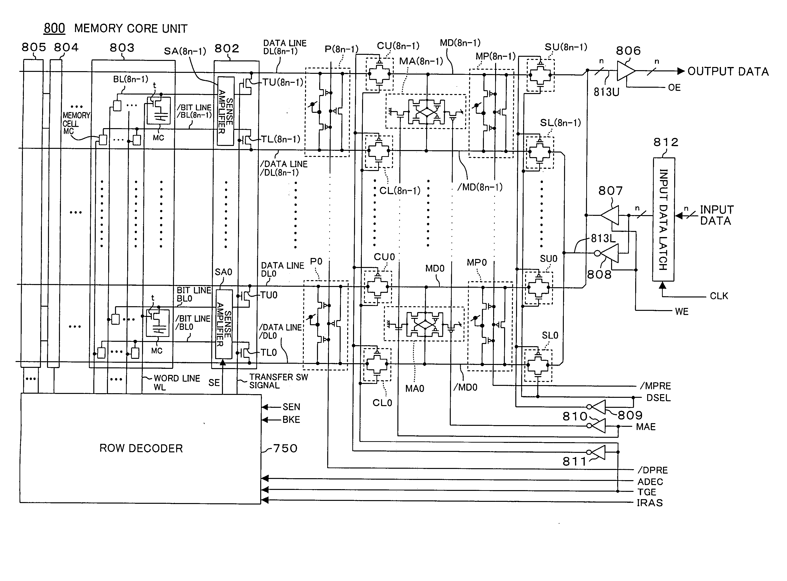
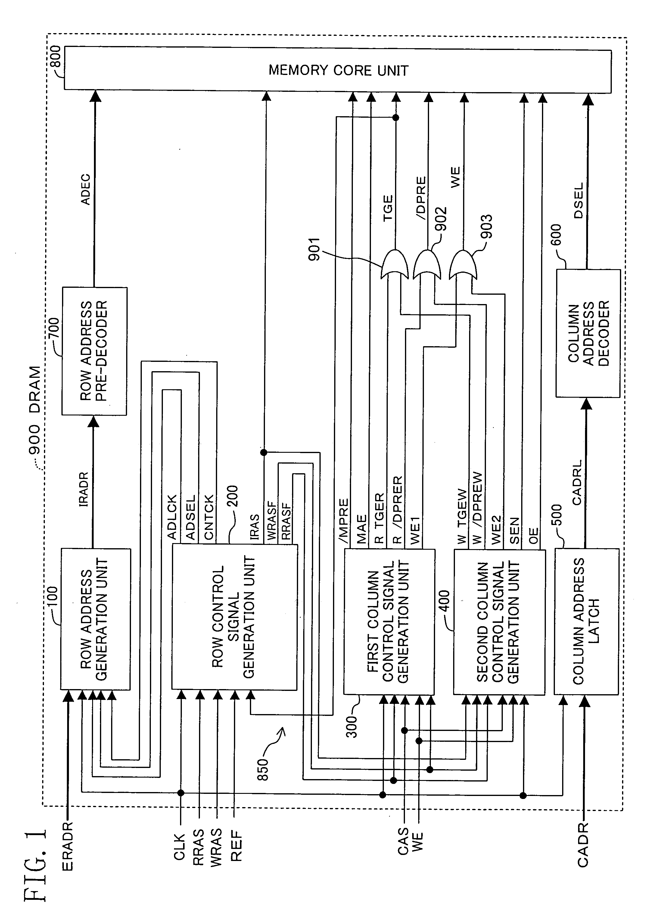
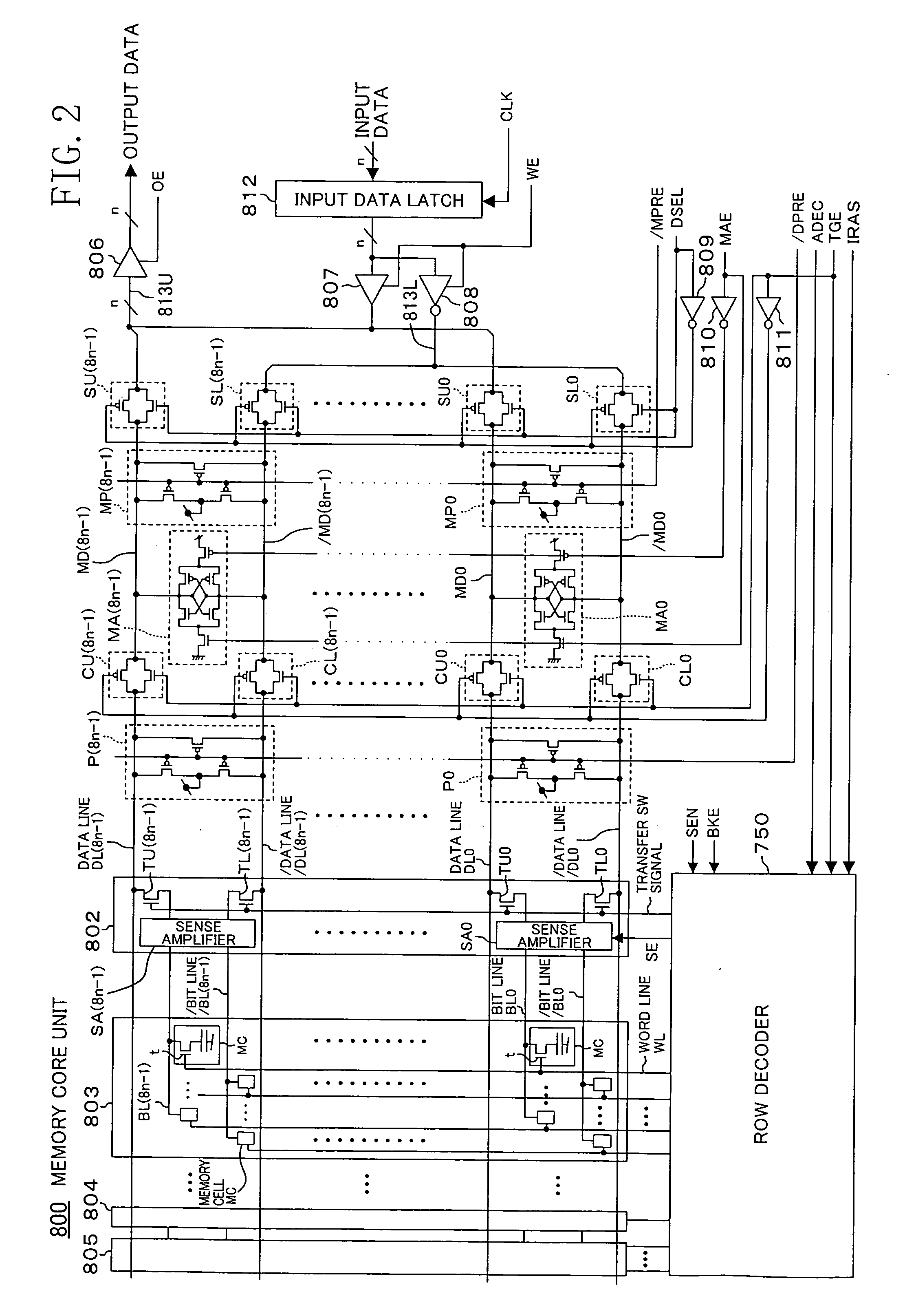
[0054]FIG. 1 shows the architecture of the DRAM 900. In FIG. 1, the DRAM 900 includes a row address generation unit 100, a row control signal generation unit 200, a first column control signal generation unit 300, a second column control signal generation unit 400, a column address latch 500, a column address decoder 600, a row address pre-decoder 700 and a memory core unit 800.

[0055] The row address generation unit 100 receives, as shown also in FIG. 4, an external row address ERADR, a clock CLK, an address latch clock ADLCK described below and supplied from the row control signal generation unit 20.0, an address switching signal ADSEL and a count clock CNTCK, and generates and outputs an internal row address IRADR. Also, the row control signal generation unit 200 receives, as shown also in FIG. 3, the clock CLK, a reading row...


PUM


Abstract

According to the invention, in a semiconductor device that needs a refresh operation for storing data, data of memory cells selected in response to a row address is read to main amplifiers through bit line pairs, sense amplifiers and data line pairs in a page-mode read operation. Thereafter, while outputting the data held in the main amplifiers to the outside, connecting transistors are turned off so as to disconnect the main amplifiers from the memory cells, and thus, the memory cells can be precharged. Also, in a page-mode write operation, while writing externally supplied input data in the main amplifiers, the memory cells can be precharged.

Description

CROSS REFERENCE TO RELATED APPLICATIONS [0001] This Non-provisional application claims priority under 35 U.S.C. § 119(a) on Patent Application No. 2003-319629 filed in Japan on Sep. 11, 2003, the entire contents of which are hereby incorporated by reference. BACKGROUND OF THE INVENTION [0002] The present invention relates to a semiconductor device equipped with a memory cells that need a refresh operation for storing data. [0003]FIG. 12 shows the architecture of a conventional DRAM. In FIG. 12, a memory cell array 1001 includes a large number of memory cells arranged in a row direction and a column direction; a plurality of pairs of bit lines connected to these memory cells and extending in the column direction; a plurality of sense amplifiers arranged in the row direction for amplifying data on these bit line pairs; and 8n pairs of data lines 1001a arranged in the column direction. Also, a ⅛ selection circuit 1002 selects n pairs of data lines 1001a from the 8n pairs of data lines....

Claims


Application Information

Patent Timeline
IPC IPC(8): G11C7/12G11C11/409G11C11/406G11C11/407G11C11/408G11C11/4094
CPCG11C7/12G11C11/406G11C2207/005G11C2207/002G11C11/4094
Inventor FUJIMOTO, TOMONORIOHTA, KIYOTOKIKUKAWA, HIROHITO
Owner CETUS TECH INC
Why Eureka
Try Eureka