

Nanotube films and articles
a technology of carbon nanotubes and nanotubes, applied in the direction of carbonsing rags, electrostatic/electro-adhesion relays, digital storage, etc., can solve the problems of non-continuous, inconvenient use, and inability to meet the needs of electrical interconnects in semiconductor devices, etc., and achieve the effect of nanotube growth
- Summary
- Abstract
- Description
- Claims
- Application Information
AI Technical Summary
Benefits of technology
Problems solved by technology
Method used
Image

Examples
Embodiment Construction
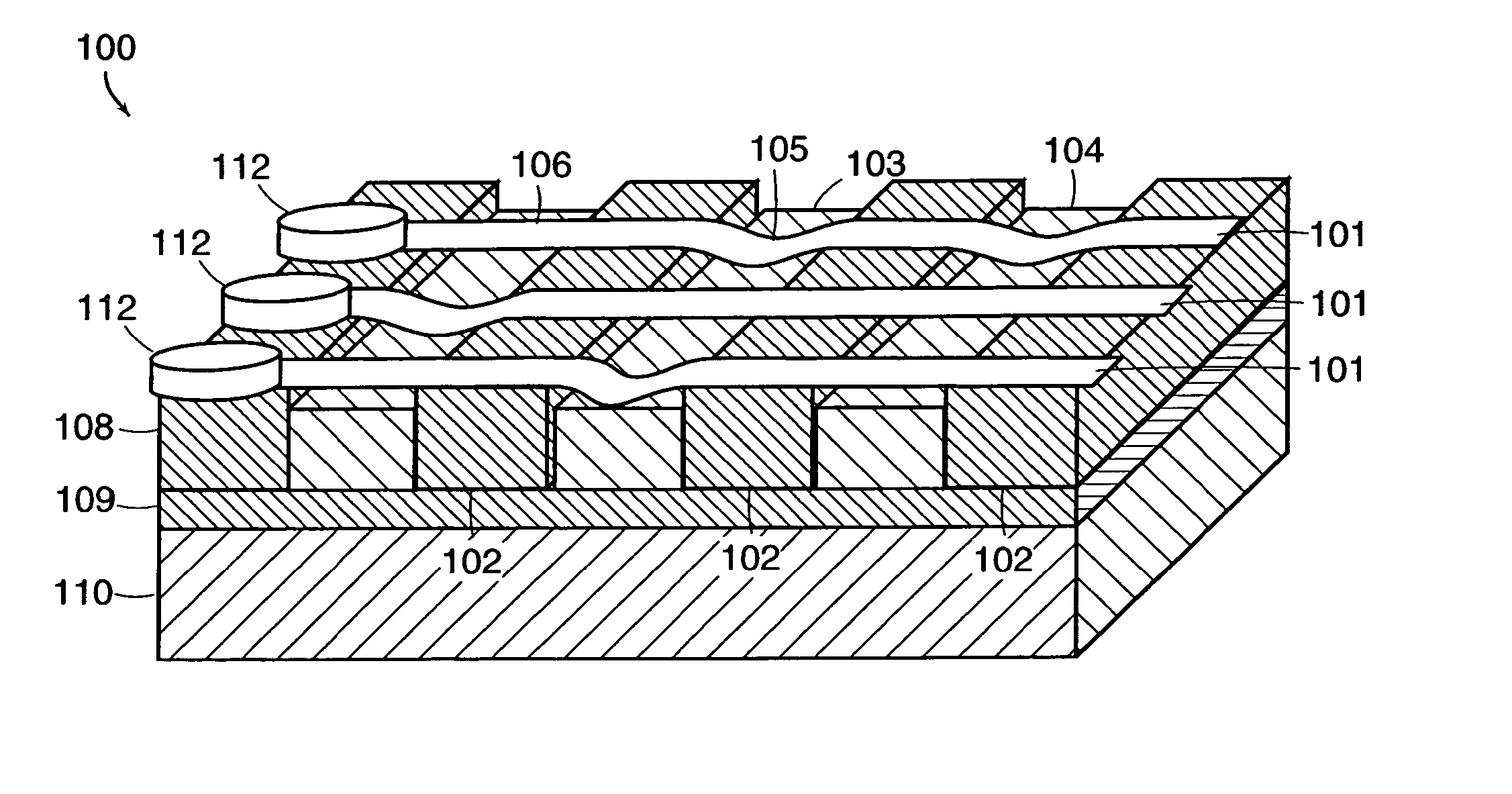
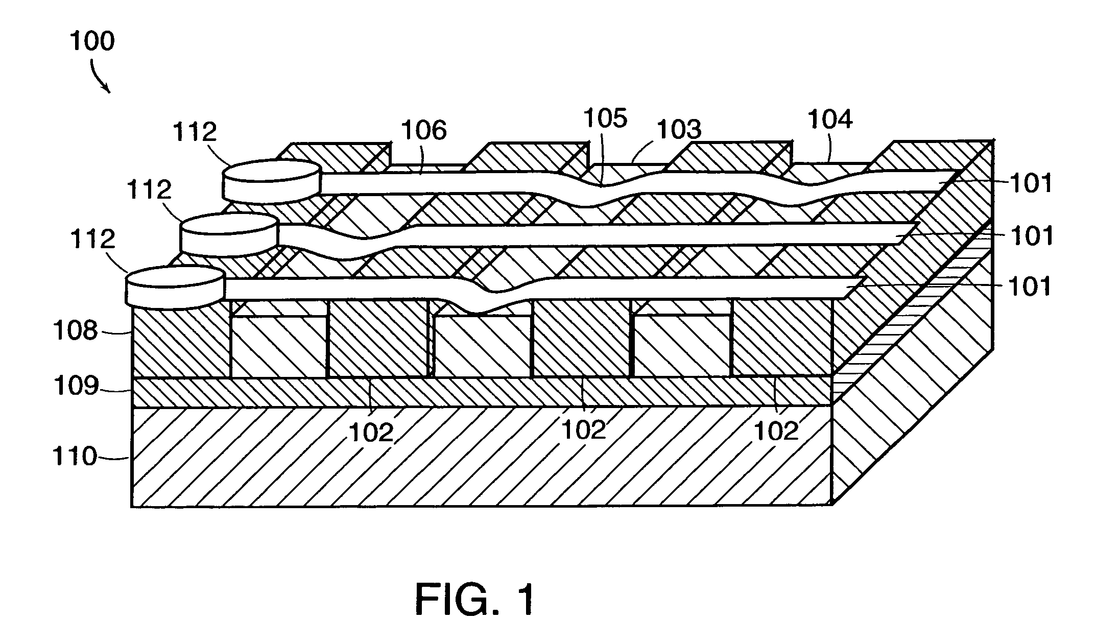
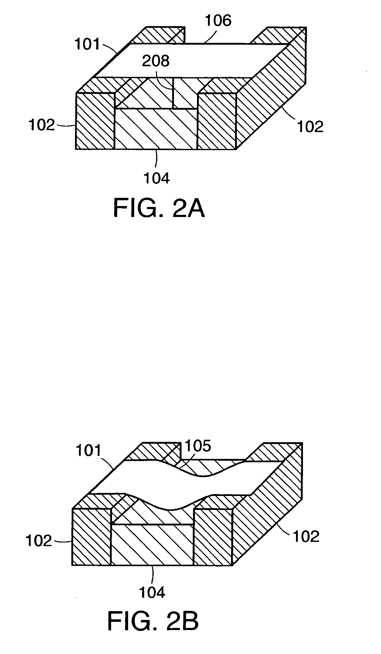
[0040] New electromechanical memory arrays and methods for making same are disclosed in which electromechanical memory cells are created that operate analogously to the NTWCM devices disclosed in WO 01 / 03208, which is hereby incorporated by reference in its entirety. However, unlike the NTWCM devices disclosed in WO 01 / 03208, new ribbons or belts made from a matted layer of nanotubes or a non-woven fabric of nanotubes are used as an electrically conductive element. At points in this disclosure, the ribbons are referred to as traces or electrically conductive articles. In some instances, the ribbons are suspended, and in other instances they are disposed on a substrate. In some instances, they are used to deflect to certain states under electrical control, and in other instances they do not move and instead are used simply to carry an electrical current or voltage. The new nanotube belt structures are believed to be easier to build at the desired levels of integration and scale (in n...
PUM
| Property | Measurement | Unit |
|---|---|---|
| diameters | aaaaa | aaaaa |
| width | aaaaa | aaaaa |
| temperature | aaaaa | aaaaa |
Abstract
Description
Claims
Application Information