Wiring repair apparatus

a technology for wiring repair and wiring, applied in the direction of manufacturing tools, instruments, and semiconductor/solid-state device details, can solve the problems of inability to completely avoid defects with any current advanced technology, and the wiring of tfts and theirs is more frequently shorted and broken, so as to achieve efficient repair of wiring, without reducing its quality and reliability

Inactive Publication Date: 2005-03-24
LASERFRONT TECH
View PDF7 Cites 9 Cited by
  • Summary
  • Abstract
  • Description
  • Claims
  • Application Information

AI Technical Summary

Benefits of technology

[0023] According to the present invention, this wiring repair apparatus, which has the CVD gas units and supplies the diffe...

Problems solved by technology

As LCDs have recently become larger, defects such as shorts and breaks occur more frequently in the wiring of integrated circuits, including TFTs and their peripheries.
Such defects cannot be completely avoided with any current advanced technology.
The above conventional technique, however, has the following problem.
Such repaired parts, having non-uniform electrical conductivity and non-uniform thermal expansivity, cause thermal stress when a heat load is applied.
The repaired wiring therefore has the disadvantage of reliabi...

Method used


Image

  • Wiring repair apparatus
  • Wiring repair apparatus
  • Wiring repair apparatus

Examples


Embodiment Construction

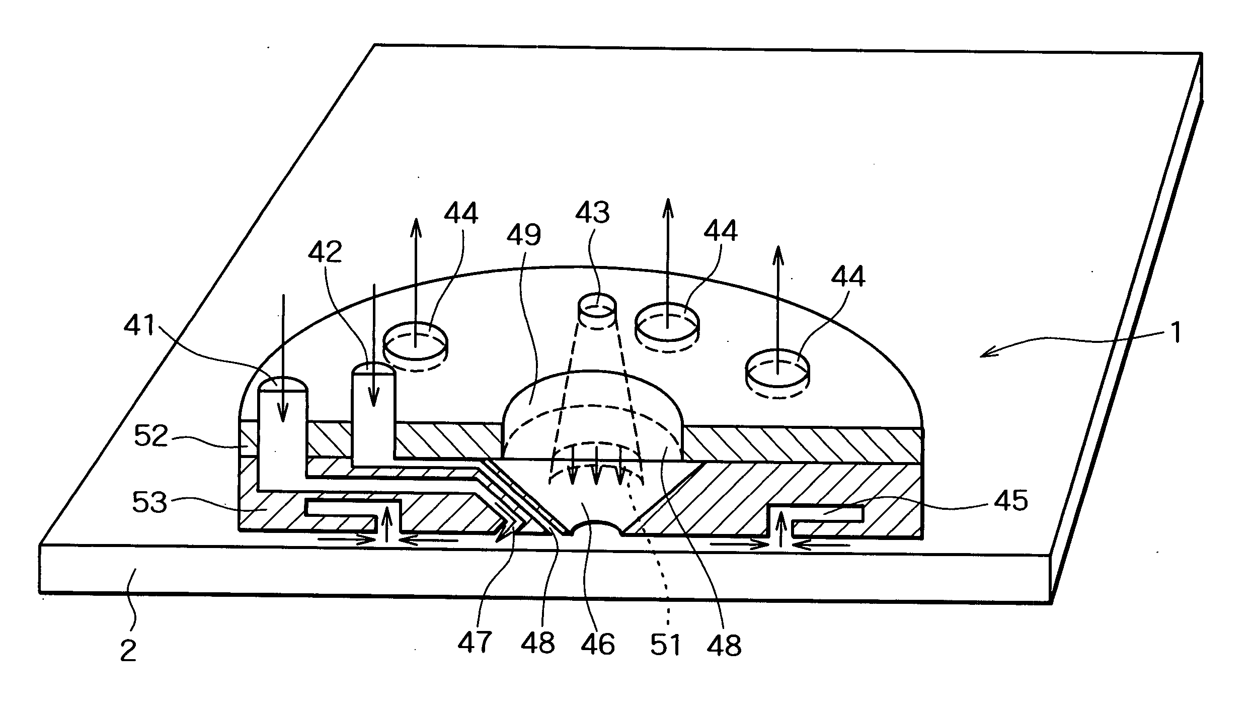
[0030] An embodiment of the present invention will now be specifically described with reference to the accompanying drawings. FIG. 3 is a schematic diagram of a wiring repair apparatus according to an embodiment of the present invention. FIG. 4 is a schematic diagram of a laser source unit and its periphery in the wiring repair apparatus shown in FIG. 3. FIG. 5 is a sectional perspective view of a gas window shown in FIG. 3. The wiring repair apparatus according to this embodiment is a laser CVD apparatus.

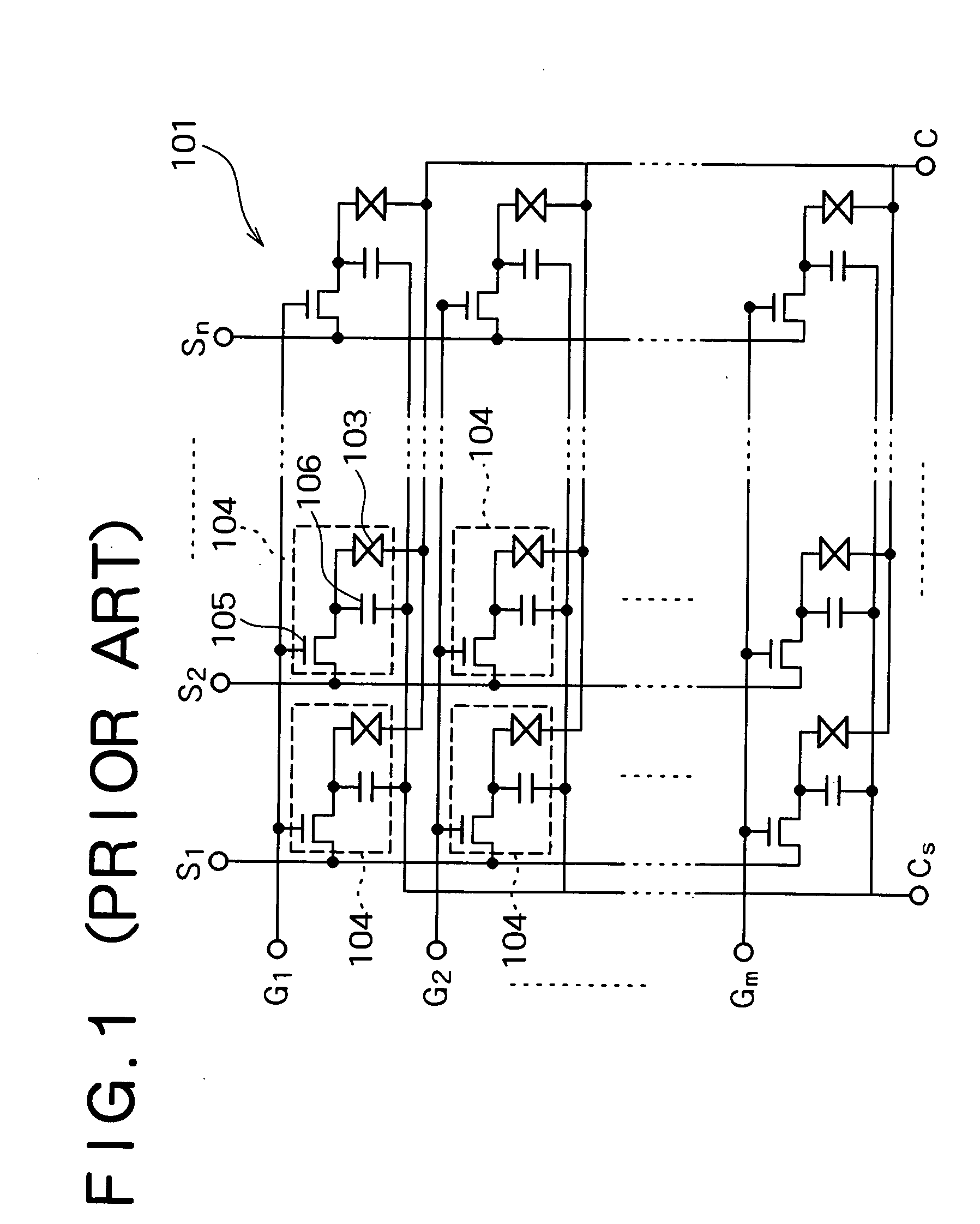
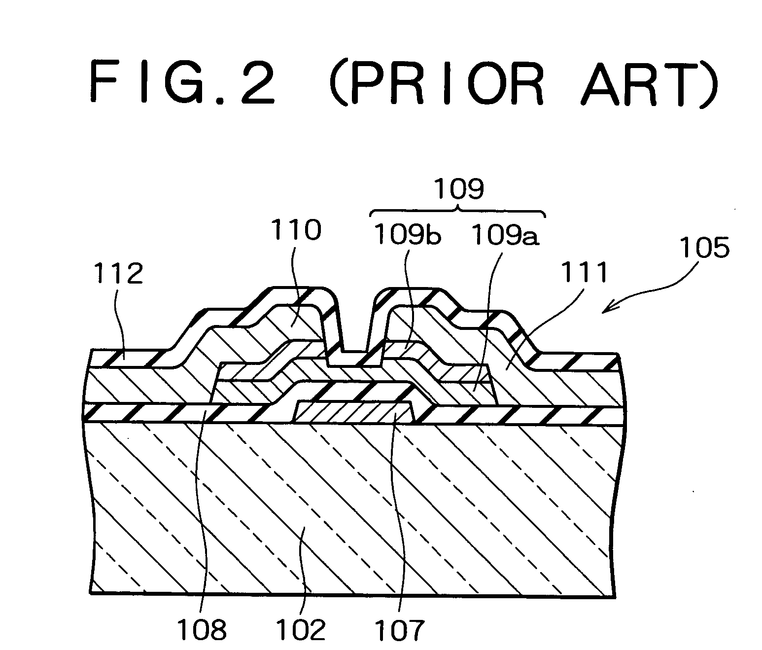
[0031] As shown in FIG. 3, a wiring repair apparatus 31 according to this embodiment includes an XY stage 17 onto which a substrate 2 to be repaired is placed. This substrate 2 is, for example, a glass substrate of an LCD as shown in FIGS. 1 and 2, and has TFTs, Al gate lines, and Cr source lines on its surface. The XY stage 17 freely moves the substrate 2 in horizontal directions, namely the X and Y directions.

[0032] A laser source unit 32 is provided above the XY stage 17 with ...


PUM

PropertyMeasurementUnit
Wavelengthaaaaaaaaaa

Abstract

A wiring repair apparatus includes an XY stage on which a substrate is placed, a laser source unit disposed above the XY stage, first and second gas windows disposed between the laser source unit and the XY stage, and first and second CVD gas units. The laser source unit emits a laser beam to a part of the substrate to be repaired. This laser beam passes through either the first or second gas window. The first CVD gas unit supplies an Al source gas (DMAH gas) to the first gas window while the second CVD gas unit supplies a Cr source gas (Cr(CO)6 gas) to the second gas window.

Description

BACKGROUND OF THE INVENTION [0001] 1. Field of the Invention [0002] The present invention relates to wiring repair apparatuses for repairing defective parts of wiring formed on a substrate and, particularly, it relates to a wiring repair apparatus for repairing breaks in wiring by laser chemical vapor deposition (CVD). [0003] 2. Description of the Related Art [0004] Liquid crystal displays (LCDS) have become rapidly widespread over the past several years. This trend is being driven by LCDs based on semiconductor thin-film transistor (TFT) technology. There are two types of TFTs: amorphous silicon (a-Si) TFTs and polysilicon (poly-Si) TFTs. These two types of TFTs have similar principles and structures. As LCDs have recently become larger, defects such as shorts and breaks occur more frequently in the wiring of integrated circuits, including TFTs and their peripheries. [0005]FIG. 1 is an equivalent circuit diagram of an LCD. FIG. 2 is a partial sectional view of a TFT in the LCD. In ...

Claims


Application Information

Patent Timeline
IPC IPC(8): G02F1/13C23C16/04C23C16/44C23C16/455C23C16/48G02F1/1343H01L21/3205H01L23/52H01L29/786
CPCC23C16/047C23C16/45519H01L2924/0002H01L2924/00G02F1/13
Inventor WAKABAYASHI, KOJI
Owner LASERFRONT TECH
Why Eureka
Try Eureka