Electron emitter

Inactive Publication Date: 2005-03-24
NGK INSULATORS LTD
View PDF5 Cites 5 Cited by
  • Summary
  • Abstract
  • Description
  • Claims
  • Application Information

AI Technical Summary

Benefits of technology

[0007] It is an object of the present invention to provide an electron emitter having an electric field receiving member made of a dielectric material in which excessive emission of elec

Problems solved by technology

All of these disclosed electron emitters are disadvantageous in that since no dielectric body is employed in the electric field receiving member, a forming process or a micromachining process is required between facing electrodes, a high voltage needs to be applied between the electrodes to emit electrons

Method used


Image

  • Electron emitter
  • Electron emitter
  • Electron emitter

Examples


first embodiment

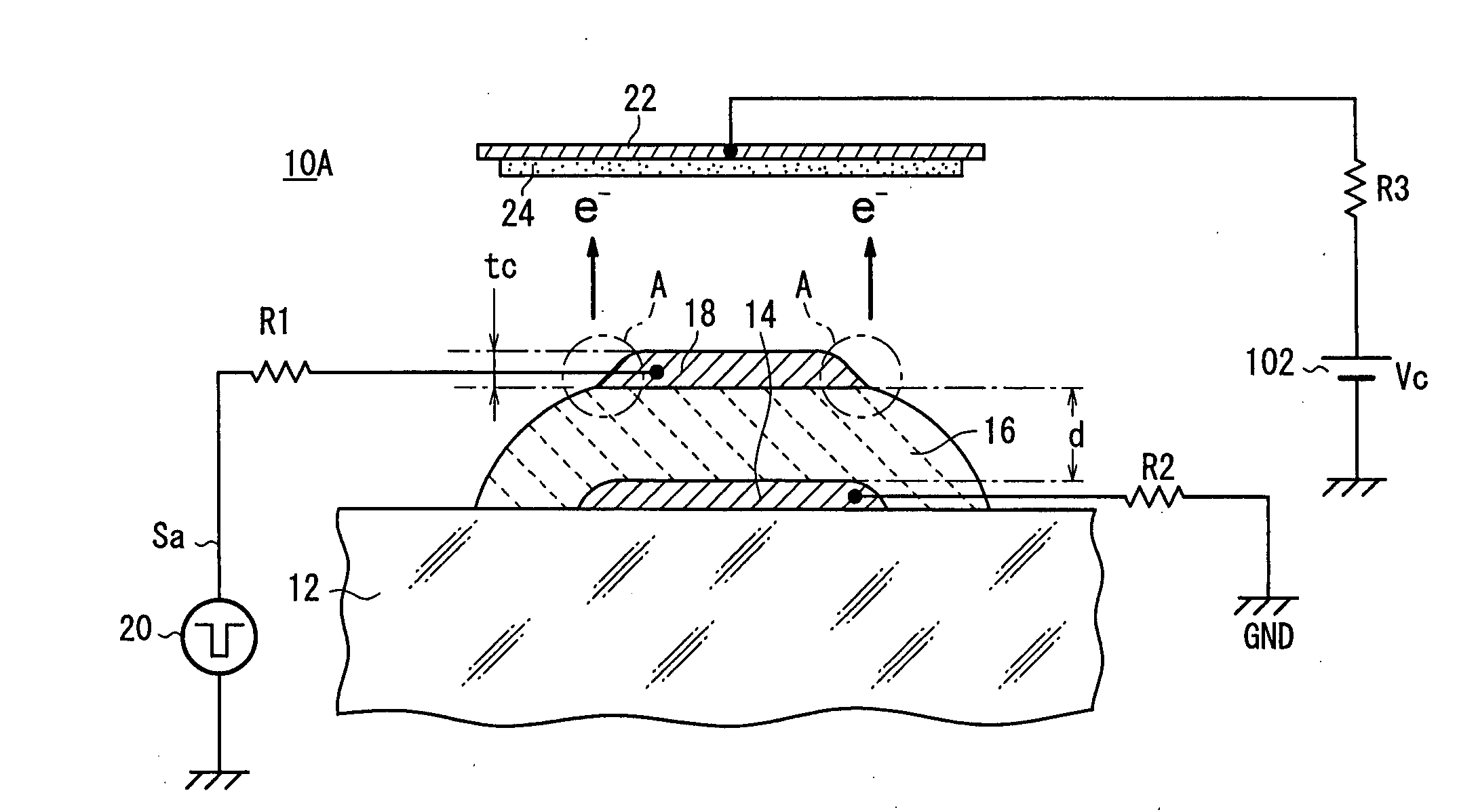
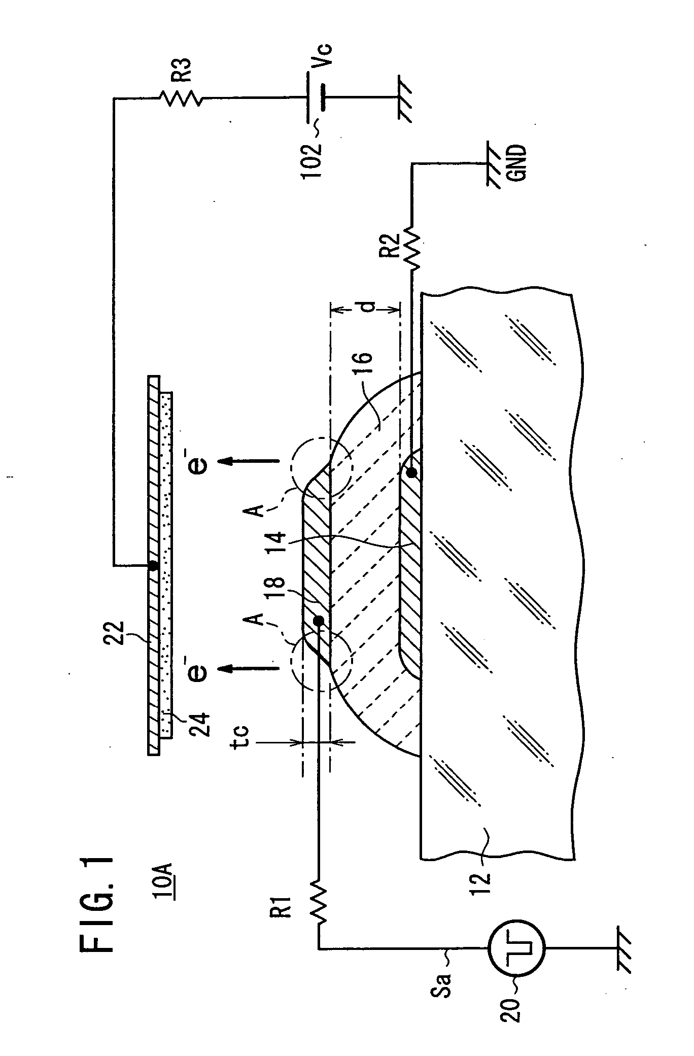
[0048] As shown in FIG. 1, an electron emitter 10A has an anode electrode 14 formed on a substrate 12, and an electric field receiving member 16 formed on the substrate 12 to cover the anode electrode 14, and a cathode electrode 18 formed on the electric field receiving member 16.

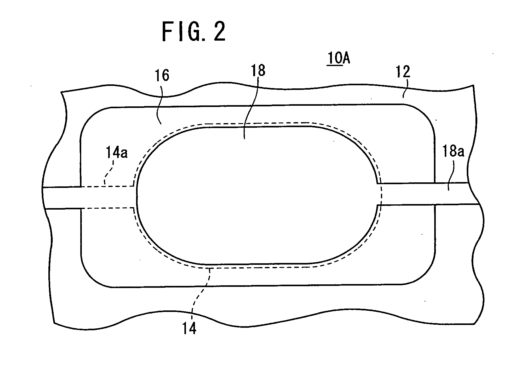
[0049] The cathode electrode 18 is supplied with a drive signal Sa from a pulse generation source 20 through a resistor R1, and the anode electrode 14 is connected to an anode potential generation source (GND in this example) through a resistor R2. As shown in FIG. 2, for example, the drive signal Sa is supplied to the cathode electrode 18 through a lead electrode 18a extending from the cathode electrode 18. The anode potential (Vss) is applied to the anode electrode 14 through a lead electrode 14a extending from the anode electrode 14.

[0050] For using the electron emitter 10A as a pixel of a display, a collector electrode 22 is positioned above the cathode electrode 18, and the collector electrode 22 is ...

second embodiment

[0101]FIG. 11 is a view showing an electron emitter 10B according to the present invention. The electron emitter 10B includes a protective film 30 formed on the electric field receiving member 16 to cover the cathode electrode 18. The protective film 30 formed on the surface of the electric field receiving member 18 prevent the electric field receiving member 16 from being damaged due to the electrons emitted from the cathode electrode 18 toward the electric field receiving member 16. Further, even if ionization occurs due to the electron emission, the protective film 30 reduces the damages of the cathode electrode 18 by the positive ions.

[0102]FIG. 12 is a view showing an electron emitter 10Ba of a first modification. The electron emitter 10Ba has a protective film 30 made of a conductor. The protective film 30 is likely to be eroded by the emitted electrons. The conductor should have a small sputtering yield (the number of target atoms or molecules per one incident ion). Preferabl...


PUM


Abstract

An electron emitter has an anode electrode formed on a substrate, an electric field receiving member formed on the substrate to cover the anode electrode, and a cathode electrode formed on the electric field receiving member. The cathode electrode is supplied with a drive signal from a pulse generation source, and the anode electrode is connected to an anode potential generation source (GND in this example). A collector electrode is provided above the cathode electrode, and the collector electrode is coated with a fluorescent layer. The collector electrode is connected to a collector potential generation source (Vc in this example) through a resistor.

Description

BACKGROUND OF THE INVENTION [0001] 1. Field of the Invention [0002] The present invention relates to an electron emitter including a cathode electrode, an anode electrode and an electric field receiving member interposed between the cathode electrode and the anode electrode. The electric field receiving member is made of a dielectric material. [0003] 2. Description of the Related Art [0004] In recent years, electron emitters having a cathode electrode and an anode electrode have been used in various applications such as field emission displays (FEDs) and backlight units. In an FED, a plurality of electron emitters are arranged in a two-dimensional array, and a plurality of fluorescent elements are positioned at predetermined intervals in association with the respective electron emitters. [0005] Conventional electron emitters are disclosed in Japanese laid-open patent publication No. 1-311533, Japanese laid-open patent publication No. 7-147131, Japanese laid-open patent publication N...

Claims


Application Information

Patent Timeline
IPC IPC(8): H01J1/30H01J1/312H01J1/32
CPCB82Y10/00H01J1/32H01J1/312H01J1/30
Inventor TAKEUCHI, YUKIHISANANATAKI, TSUTOMUOHWADA, IWAO
Owner NGK INSULATORS LTD
Why Eureka
Try Eureka