Image sensing apparatus

a technology of image sensing and apparatus, applied in the field of image sensing apparatus, can solve the problems of degrading spatial resolution, reducing the number of pixels per unit area of the chip, and inevitably increasing the geometric structure (pixel size) of one pixel

Inactive Publication Date: 2005-03-24
JAPAN SCI & TECH CORP
View PDF6 Cites 13 Cited by
  • Summary
  • Abstract
  • Description
  • Claims
  • Application Information

AI Technical Summary

Problems solved by technology

With the vision chip of the single-chip system as stated above, however, the optical sensor and the processing circuits are arranged in each pixel, so that the geometrical structure (pixel size) of one pixel enlarges inevitably.
Moreover, with the prior-art vision chip, various visual processing functions need to be incarnated by one chip, so that the number of pixels per unit area of the chip decreases to degrade a spatial resolution.
Furthermore, with the prior-art vision chip, the pixel size is made small by simplifying the pixel...

Method used


Image

  • Image sensing apparatus
  • Image sensing apparatus
  • Image sensing apparatus

Examples


Embodiment Construction

1. Multi-Chip System

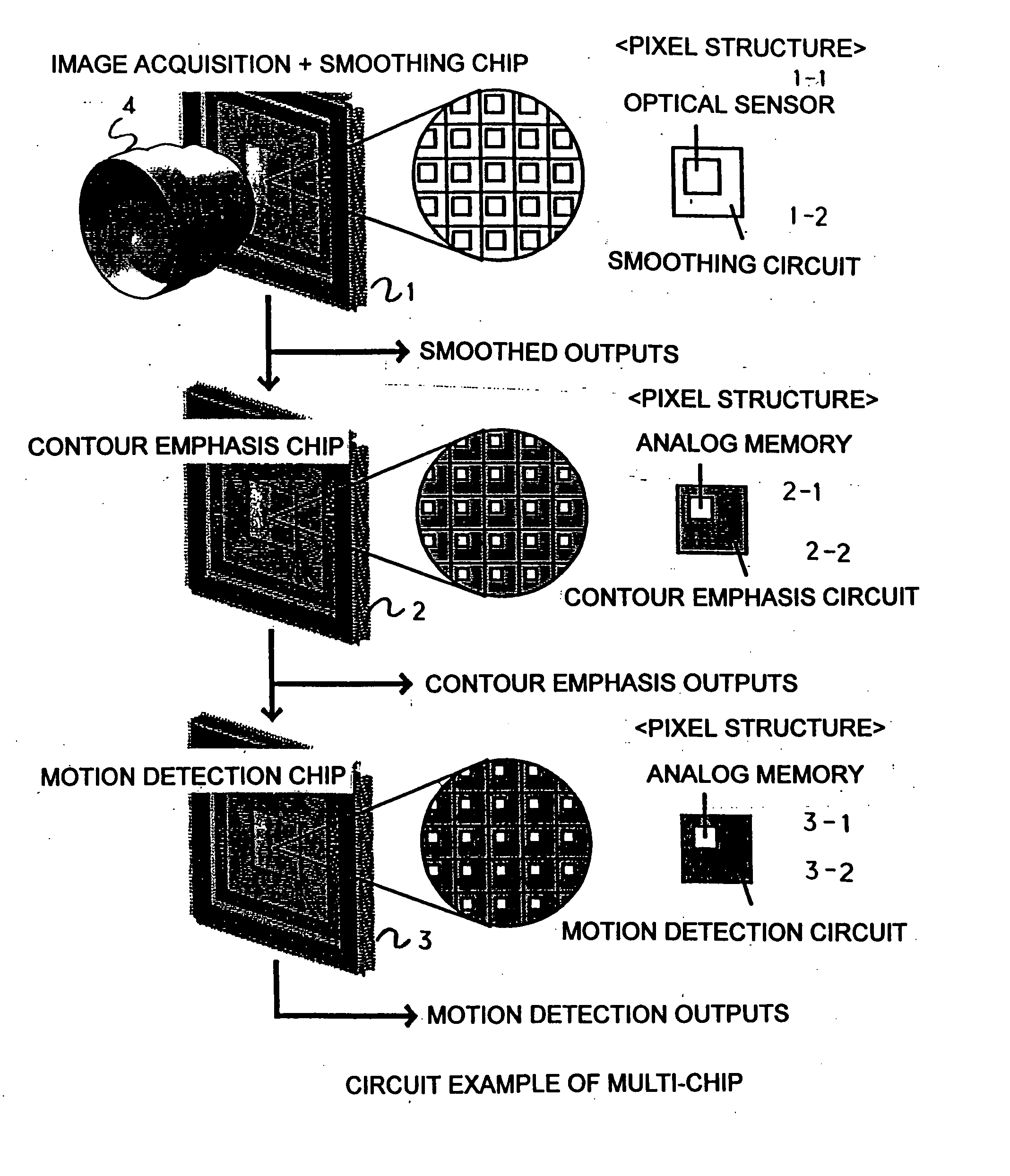
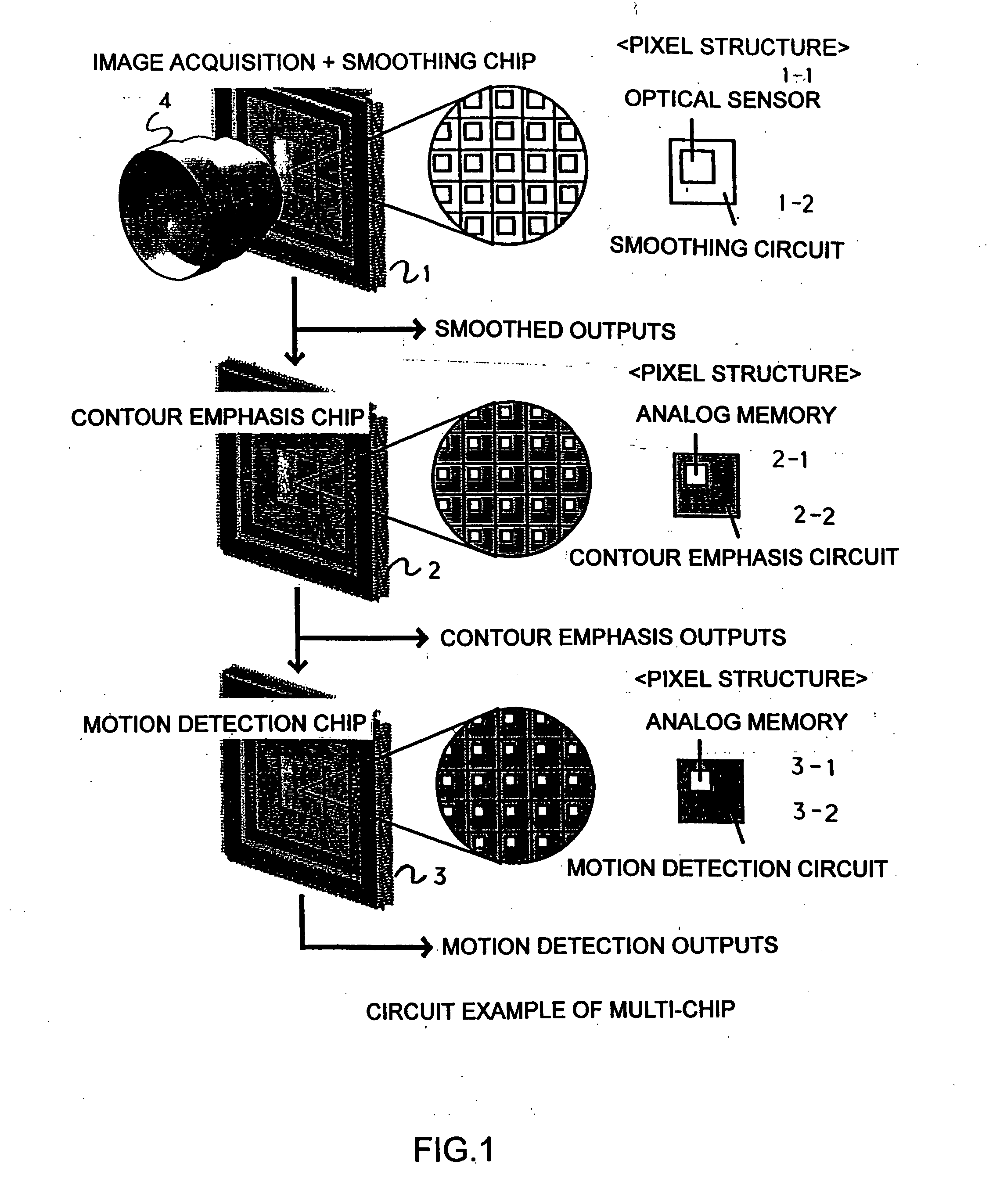
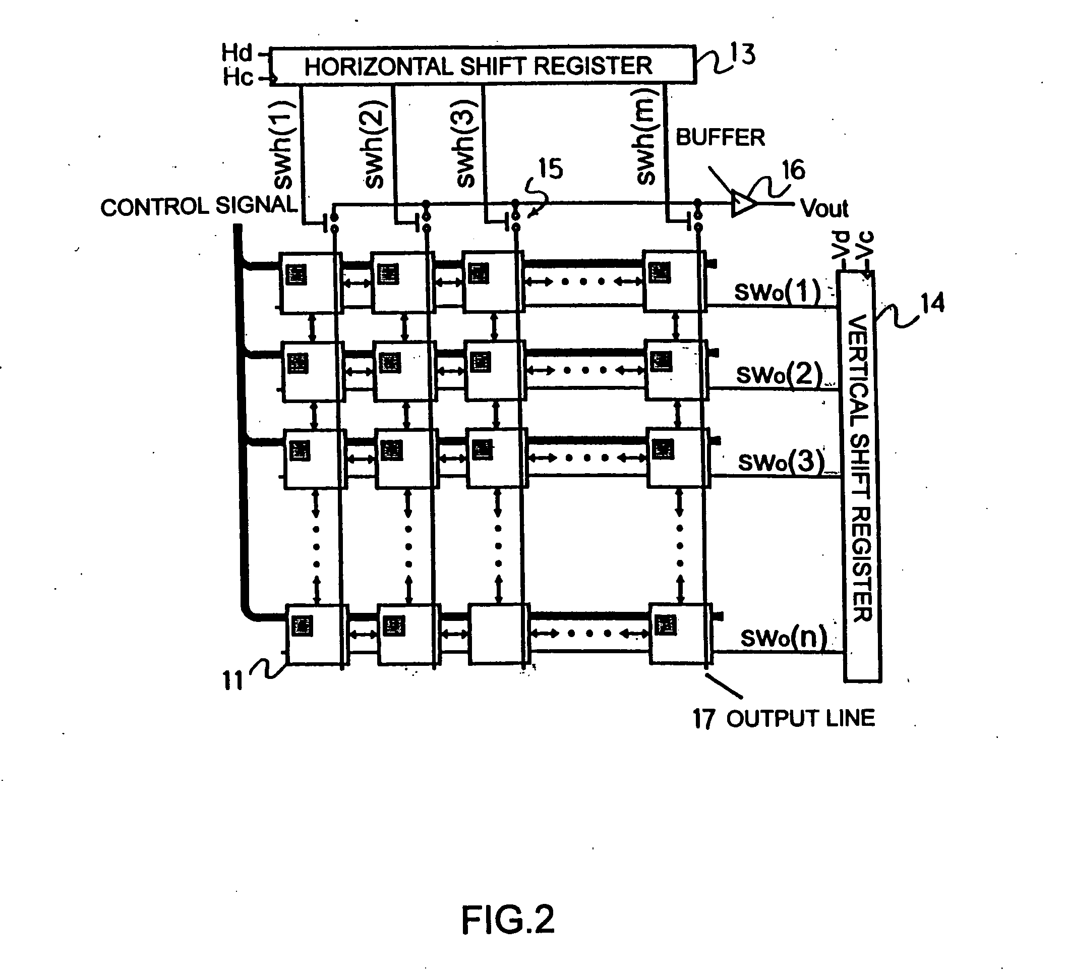
Shown in FIG. 1 is the constructional view of an image sensing apparatus being a multi-chip system. In this embodiment, by way of example, the three processing items of smoothing, contour emphasis and motion detection are respectively distributed to three chips, which are constructed into a multi-chip. The smoothing chip 1 of first stage, to which image information is inputted from an optical system 4 constructed of a lens, etc., includes an optical sensor circuit 1-1, and a smoothing circuit 1-2 which is a processing circuit for smoothing, thereby to smooth an input image. The smoothed image information is outputted as voltage or current analog signals from the first-stage smoothing chip 1, and the analog signals are inputted to the contour emphasis chip 2 and motion detection chip 3 of second stage, et seq. The pixels of the contour emphasis chip 2 and motion detection chip 3 at the second stage, et seq. include analog memories 2-1, 3-1, and a contour emphas...


PUM


Abstract

An Image sensing apparatus employing a multi-chip system and having a super-parallel circuit structure capable of performing processes such as image processing in real time. A first chip of a first of a first stage has first pixel circuits each having an optical sensor and first processing circuits and arranged in a matrix. A second chip of a second stage has second pixel circuits each having an analog memory for storing analog information from the preceding stage and second processing circuits and arranged in a matrix so as to correspond to the first pixel circuits. In each of the first and the second chip, each of the first and the second processing circuits receives an analog signal from another first and second processing circuit in the vicinity so as to perform first and second analog processing and performs circuit noise compensation by parallel calculation.

Description

BACKGROUND OF THE INVENTION The present invention relates to an image sensing apparatus, and more particularly to an image sensing apparatus called “vision chip”, which is applied to a vision sensor and image processing. Here, the “vision chip” signifies, for example, a visual sensor chip (semiconductor or circuit) in which a super-parallel circuit structure with optical sensor circuits and processing circuits arranged for individual pixels is realized by an analog CMOS integrated circuit, and which can perform visual information processing. Among such vision chips, especially a vision chip which simulates the circuit structure and functions of an organic retina shall be called “silicon retina”. Shown in FIG. 22 is the schematic constructional view of a vision chip. A lower view is the enlarged view of the vision chip 61. As in the enlarged view, each pixel includes an optical sensor 63 and a processing circuit 64. Image information is projected on the vision chip 61 through an op...

Claims


Application Information

Patent Timeline
IPC IPC(8): G06T1/20G06T1/00G06T7/20H04N5/335H04N5/351H04N5/357H04N5/369H04N5/374H04N5/3745H04N13/02
CPCH04N5/335H04N5/378H04N5/3653H04N25/00H04N25/672H04N25/75H04N25/76
Inventor YAGI, TETSUYAKAMEDA, SEIJI
Owner JAPAN SCI & TECH CORP
Why Eureka
Try Eureka