
Organic field emission device and emission device

a technology of emission device and organic field, which is applied in the direction of discharge tube/lamp details, luminescnet screen, discharge tube/lamp details, etc., to achieve the effect of improving the service life of the device and stable hu

Inactive Publication Date: 2005-03-24
SONY CORP
View PDF7 Cites 7 Cited by
  • Summary
  • Abstract
  • Description
  • Claims
  • Application Information

AI Technical Summary

Benefits of technology

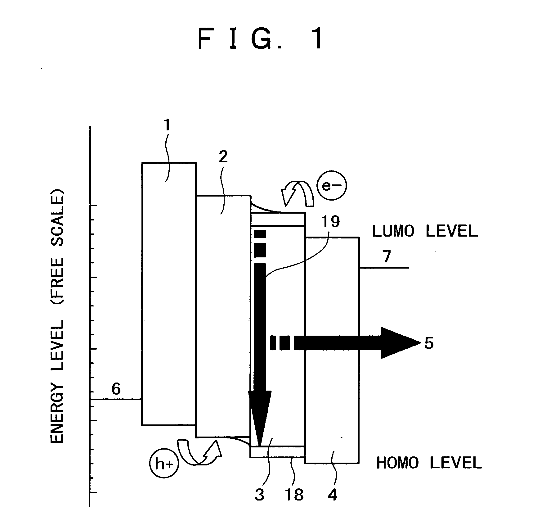
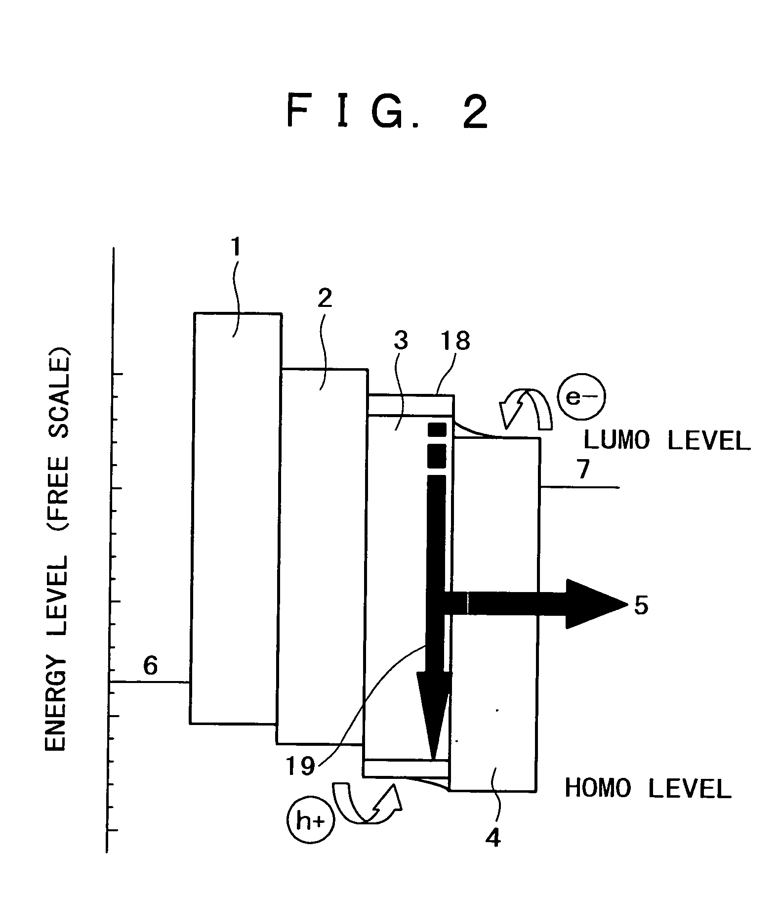
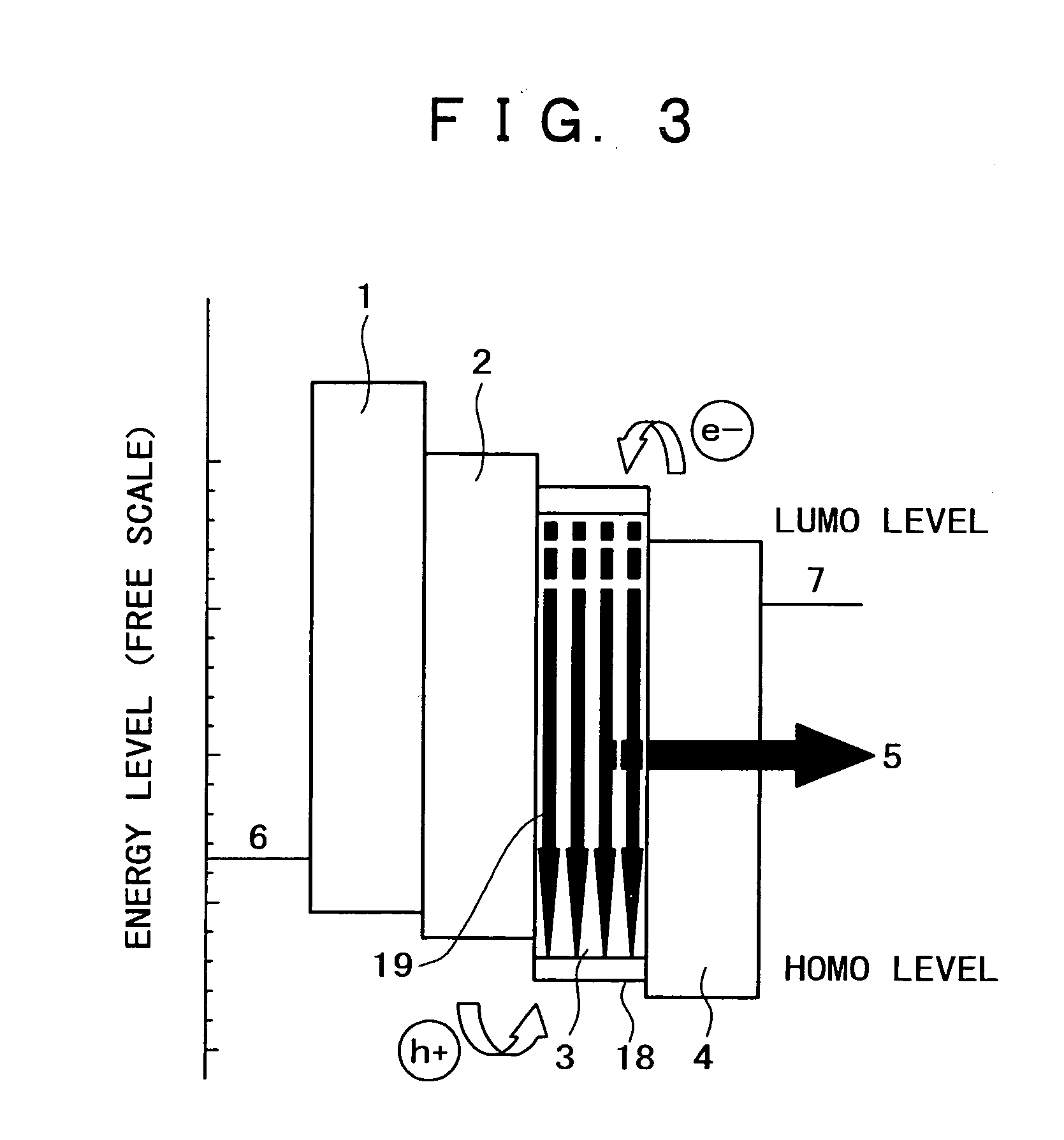
The organic electroluminescence light emitting device of the present invention typically includes an anode, a hole transport layer, a light emission layer, an electron transport layer, or includes an anode, a hole transport layer, and a light emission layer serving as an electron transport layer. A light emission region of the device is formed by a mixed layer made from a luminescent material and a charge injection accelerating material. The luminescent material exhibits, in a state held as a single thin film between the anode and the cathode, electroluminescence light emission when a DC voltage is applied thereto and has a charge transport characteristic. The charge injection accelerating material is different from the luminous material and has a charge transport characteristic capable of accelerating injection of charges in the luminescent material. The light emission region exists not only at an interface with an adjacent layer or its vicinity but also over a specific thickness region in the layer thickness direction. Accordingly, a region in which light is emitted is not limited to the above-described interface or its vicinity but can be spread in a wide range of the light emission layer. This means that even if the performance of a portion located in the layer thickness direction is deteriorated, light emission occurs a portion above or below the deteriorated portion, so that light emission occurs substantially over a specific thickness region in the light emission layer. As a result, it is possible to significantly improve the service life of the device.

Problems solved by technology

This means that even if the performance of a portion located in the layer thickness direction is deteriorated, light emission occurs a portion above or below the deteriorated portion, so that light emission occurs substantially over a specific thickness region in the light emission layer.

Method used


Image

  • Organic field emission device and emission device
  • Organic field emission device and emission device
  • Organic field emission device and emission device

Examples


example 1

Concentration of Compound 1 and Luminous Efficiency

In this example, organic electroluminescence light emitting devices, each using, as a light emission layer having an electron transport characteristic, a mixed layer made from a styryl compound represented by a compound 1 described below and an electron transport material represented by Alq3 (tris (8-quinolinol) aluminum) described below, are produced as samples, and a relationship between a luminance of light emitted from each sample and a luminous efficiency of the sample is examined.

Samples of organic electroluminescence light emitting devices were prepared as follows: namely, as a light emission layer of each organic electroluminescence light emitting device, a mixed layer made from a styryl compound 1 expressed by the following chemical formula, and an electron transport material Alq3 expressed by the following chemical formula was formed by a vacuum vapor-deposition process; and as the other components of this light emitti...

example 2

Concentration of Compound 1 and Luminous Efficiency

In this example, organic electroluminescence light emitting devices, each using, as a light emission layer having a hole transport characteristic, a mixed layer made from the same styryl compound 1 as that described in Example 1 and the same hole transport material α-NPD as that described in Example 1, are produced as samples, and a relationship between a luminance of light emitted from each sample and a luminous efficiency of the sample is examined.

Samples of organic electroluminescence light emitting devices were prepared in the same manner as that described in Example 1, except that a mixed layer made from the same styryl compound 1 as that described in Example 1 and the same hole transport material α-NPD as that described in Example 1 was formed as a light emission layer by a vacuum vapor-deposition process.

[Device Structure]: Device (2-1): ITO / α-NPD [30 nm] / compound 1:α-NPD=1:9 [30 nm] / Alq3 [30 nm] / Mg:Ag [200 nm] Device...

example 3

Concentration of Compound 2 and Luminous Efficiency

In this example, organic electroluminescence light emitting devices, each using, as a light emission layer having an electron transport characteristic, a mixed layer made from a styryl compound represented by a compound 2 described below and the same electron transport material Alq3 (tris (8-quinolinol) aluminum) as that described in Example 1, are produced as samples, and a relationship between a luminance of light emitted from each sample and a luminous efficiency of the sample is examined.

Samples of organic electroluminescence light emitting devices were prepared in the same manner as that described in Example 1, except that a mixed layer made from a styryl compound represented by a compound 2 expressed by the following chemical formula and the same electron transport material Alq3 as that described in Example 1 was formed as a light emission layer by a vacuum vapor-deposition process.

[Device Structure]: Device (3-1): IT...


PUM

PropertyMeasurementUnit
Fractionaaaaaaaaaa
Fractionaaaaaaaaaa
Fractionaaaaaaaaaa

Abstract

The present invention provides an organic electroluminescence light emitting device capable of preventing a color (hue) of light and a luminous efficiency from being varied depending on a concentration of a luminous material contained in a light emission layer and an operational condition such as an applied voltage, thereby exhibiting a high luminance, a high performance, and a stable, reliability. The light emitting device includes an anode (6), a hole transport layer (2), a light emission layer (3), an electron transport layer (4), or includes an anode (6), a hole transport layer (2), and a light emission layer (4) serving as an electron transport layer. A light emission region is formed by a mixed layer made from a luminescent material and a charge injection accelerating material. The luminescent material exhibits, in a state held as a single thin film between the anode (6) and the cathode (7), electroluminescence light emission when a DC voltage is applied thereto and has a charge transport characteristic. The charge injection accelerating material is different from the luminous material and has a charge transport characteristic capable of accelerating injection of charges in the luminescent material. The light emission region exists not only at an interface with an adjacent layer or its vicinity but also over a specific thickness region in the layer thickness direction.

Description

TECHNICAL FIELD The present invention relates to an organic electroluminescence light emitting device (organic EL device) including an organic layer having a light emitting region between an anode and a cathode, and to a light emitting apparatus, such as a display device, using the same. BACKGROUND ART Displays have a major role in our daily living, for example, in the forms of television receivers, computer monitors, and portable information terminals. With advance of the Internet, displays as human interfaces have become increasingly important. These displays have been required to have a screen being comfortable for eyes to see and ensuring a definition high enough to allow clear viewing, and to have a resolution and a responsiveness high enough to allow clear, clean viewing of moving pictures without delay. Organic EL devices using organic compounds as luminescent materials exhibit a wide viewing angle, a high contrast, and an excellent visibility. Another advantage of organic...

Claims


Application Information

Patent Timeline
IPC IPC(8): H01L51/50
CPCH01L51/5012H10K50/11H05B33/14
Inventor ISHIBASHI, TADASHITAMURA, SHINICHIROUEDA, NAOYUKIICHIMURA, MARIYAMADA, JIRO
Owner SONY CORP
Learn More