Organic EL devices and production process thereof

Inactive Publication Date: 2005-03-24
DENSO CORP
View PDF5 Cites 87 Cited by
  • Summary
  • Abstract
  • Description
  • Claims
  • Application Information

AI Technical Summary

Benefits of technology

[0075] Furthermore, when the light-emitting layer has the laminated structure as described above, and two or more light-emitting layer each contains different light-emitting additive dyes, it could be confirmed that if a blue light-emitting layer containing a blue light-emitting additive dye is contained in the light-emitting

Problems solved by technology

However, hitherto, it was very difficult to practice the application of the organic EL device in the production of the in-vehicle display devices, because the EL device has to satisfy the highly increased standards of the qualities for the in-vehicle devices, and also it suffers from the inherent problems due to use of the organic EL materials such as reduction of the luminescence and low heat resistance.
However, the inventors of this application have found as a result of the study and examination of the proposed EL devices that some of the hole-transporting materials as the host mate

Method used


Image

  • Organic EL devices and production process thereof
  • Organic EL devices and production process thereof
  • Organic EL devices and production process thereof

Examples


example 1-1

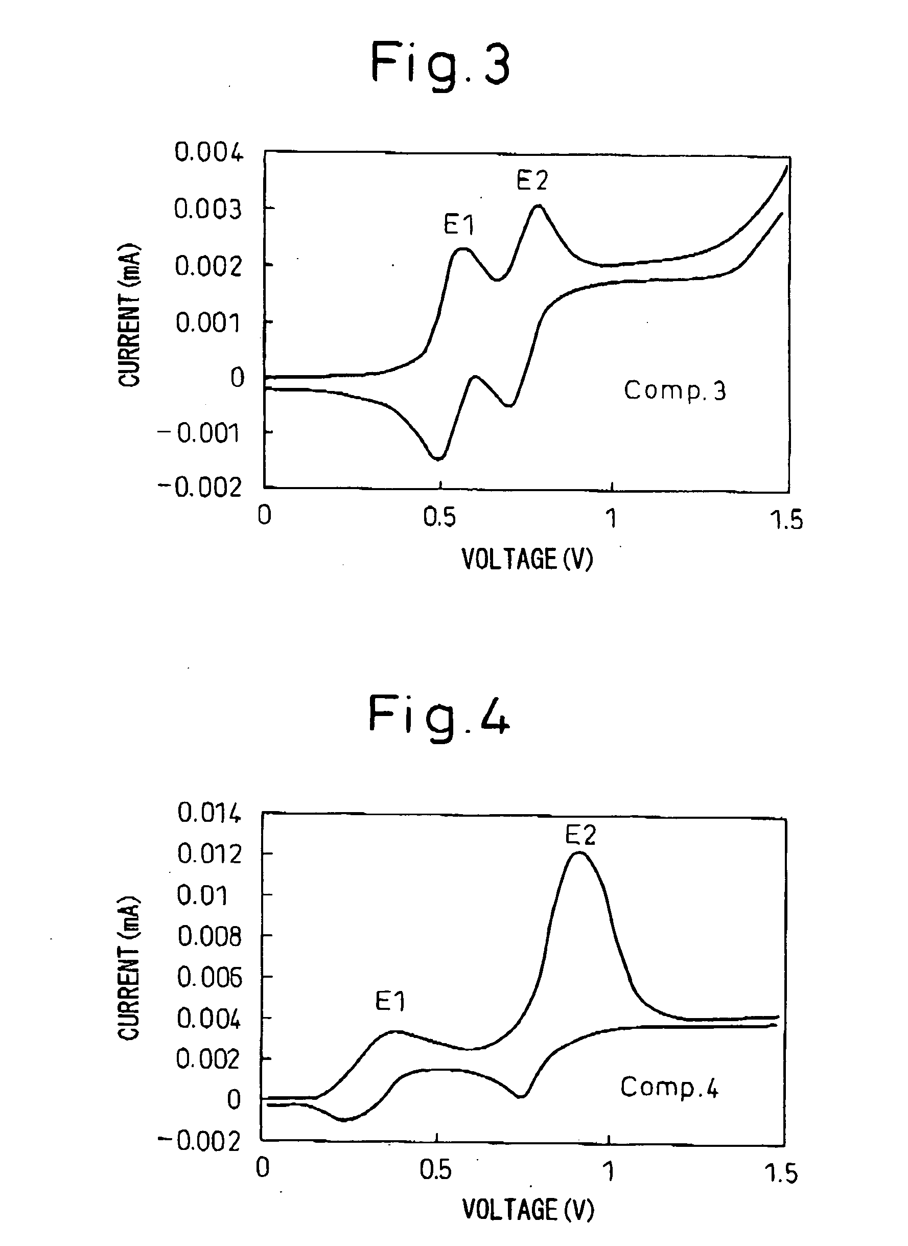
[0250] An ITO coating (transparent electrode) was formed as an anode 20 on the glass substrate 10, and a surface of the ITO coating was polished to obtain a surface roughness of Ra of about 1 nm and Rz of about 10 nm.

[0251] A hole-injecting layer 30 consisting of CuPc as an organic material having a crystallinity was formed at a thickness of 10 nm on the anode 20. Then, to form a hole-transporting layer 40, Compound 1 (tertiary amine compound) was formed at a thickness of 20 nm on the hole-injecting layer 30.

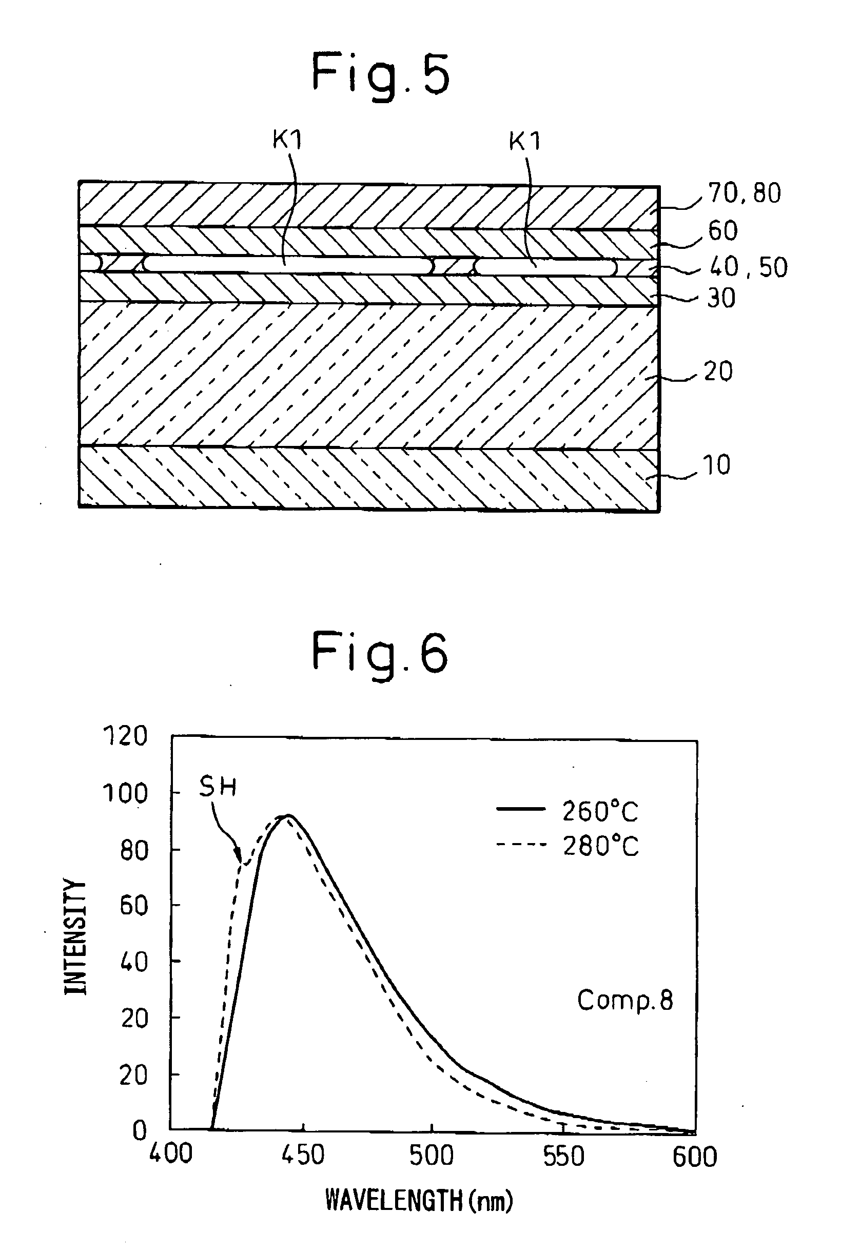
[0252] A light-emitting layer 50 was formed at a thickness of 20 nm on the hole-transporting layer 40. The light-emitting layer 50 was formed from Compound 1 (tertiary amine compound), Compound 8 (electron-transporting material) and Compound 9 (light-emitting additive material) in a weight ratio of 60:20:3. The heating temperature of Compound 8 as the electron-transporting material was adjusted to 260° C.

[0253] Thereafter, a 20 nm-thick electron-transporting layer 60 consisti...

example 1-2

[0255] The procedure of Example 1-1 was repeated with the proviso that, in the formation of the light-emitting layer 50, the heating temperature of Compound 8 (electron-transporting material) was increased to 280° C.

[0256] The EL device was subjected to the durability test under the conditions: circumstance temperature of 85° C., initial luminescence of 400 cd / m2 and 1 / 64 duty driving. The results described in Table 1 were obtained. Further, it was observed in the storage test under the circumstance temperature of 100° C. that no remarkable dark spot is generated over 500 hours.

example 2-1

[0257] The procedure of Example 1-1 was repeated with the proviso that Compound 2 was used as the tertiary amine compound in the formation of the hole-transporting layer 40 and the light-emitting layer 50.

[0258] The EL device was subjected to the durability test under the conditions: circumstance temperature of 85° C., initial luminescence of 400 cd / m2 and 1 / 64 duty driving. The results described in Table 1 were obtained. Further, it was observed in the storage test under the circumstance temperature of 100° C. that no remarkable dark spot is generated over 500 hours.


PUM

PropertyMeasurementUnit
Temperatureaaaaaaaaaa
Electric potential / voltageaaaaaaaaaa
Nanoscale particle sizeaaaaaaaaaa

Abstract

An organic electroluminescent device comprising a light-emitting layer between a pair of electrodes, the light-emitting layer comprising a mixture of a hole-transporting material consisting of a tertiary amine compound, an electron-transporting material and a light-emitting additive material, in which the tertiary amine compound has two or more oxidation potentials determined by a cyclic voltammetry wherein a potential difference between the first oxidation potential and the second oxidation potential in the oxidation potentials is 0.22V or more, and a glass transition temperature of at least 100° C., and the electron-transporting material has a glass transition temperature of at least 100° C.

Description

CROSS-REFERENCE TO RELATED APPLICATIONS [0001] This application is based upon and claims priorities of Japanese Patent Application Nos. 2003-149516, filed May 27, 2003; 2003-316872, filed Sep. 9, 2003; and 2004-41458, filed Feb. 18, 2004, the contents being incorporated herein by reference. BACKGROUND OF THE INVENTION [0002] 1. Field of the Invention [0003] The present invention relates to an organic electroluminescent (EL) device and a production process thereof. More particularly, the present invention relates to an organic EL device, in which a mixed host comprising a mixture of a hole-transporting material and an electron-transporting material is used as a host material of the light-emitting layer, and a production process of such an organic EL device. [0004] 2. Description of the Related Art [0005] The organic EL device can exhibit an excellent visibility because light is emitted based on a self-emission mechanism, and also its weight inclusive of the driving circuits can be re...

Claims


Application Information

Patent Timeline
IPC IPC(8): C09K11/06H01L51/50H01L51/00H05B33/14
CPCH01L51/0058H01L51/0059H01L51/006H01L2251/308H01L51/5012H01L51/5036H01L51/0081Y10S428/917H10K85/631H10K85/626H10K85/633H10K85/324H10K50/11H10K50/125H10K2102/103
Inventor KATO, TETSUYAKOJIMA, KAZUSHIGEKAJIOKA, TAKANORIISHII, MASAHIKO
Owner DENSO CORP
Why Eureka
Try Eureka