Mask manufacturing method

a mask manufacturing and lithography technology, applied in the field of mask manufacturing methods, can solve the problems of shortening the wavelength of laser light, affecting the quality of masks, and taking a long time, and achieve the effects of short time, fine opening, and cheap and simple manufacturing

Inactive Publication Date: 2005-03-24
CANON KK
View PDF14 Cites 18 Cited by
  • Summary
  • Abstract
  • Description
  • Claims
  • Application Information

AI Technical Summary

Benefits of technology

[0009] An object of the present invention is to provide a mask manufacturing method capable of manufactu

Problems solved by technology

While the fineness is being improved in the optical lithography, in order to assure microprocessing of 0.1 μm or narrower, there still remain many unsolved problems such as further shortening of wavelength of laser light, development of lenses usable in such wavelength region, and the like.
Thus, there is a problem that the throughput is not high.
Such an EB dr

Method used


Image

  • Mask manufacturing method
  • Mask manufacturing method
  • Mask manufacturing method

Examples


Embodiment Construction

[0028] Hereinbelow, embodiments of the mask manufacturing method according to the present invention will be described.

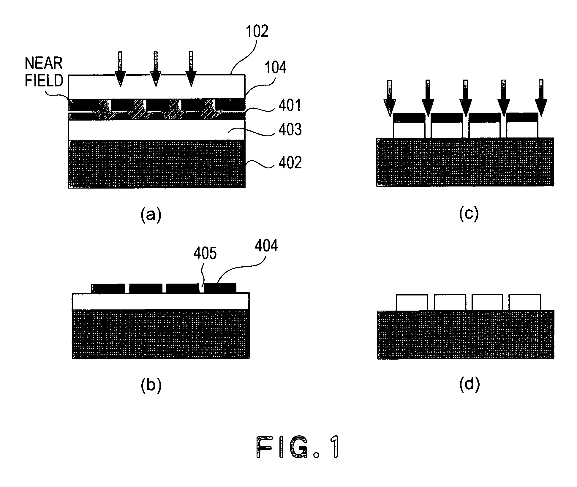
[0029] Herein, a mask as an original (original mask) is referred to as a “first mask”, and a mask manufactured on the basis of a fine pattern formed with the first mask through near-field exposure is referred to as a “second mask”.

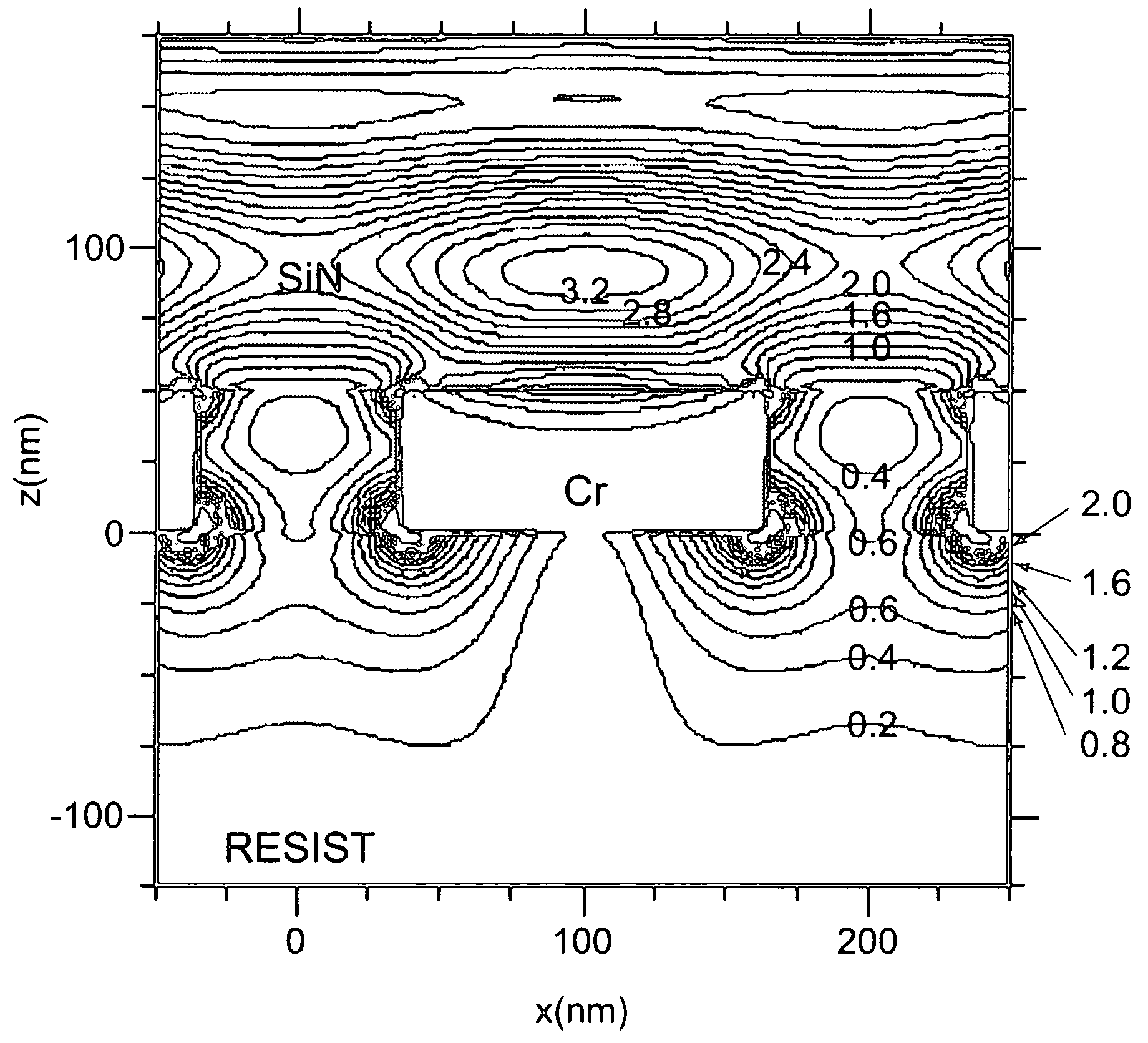
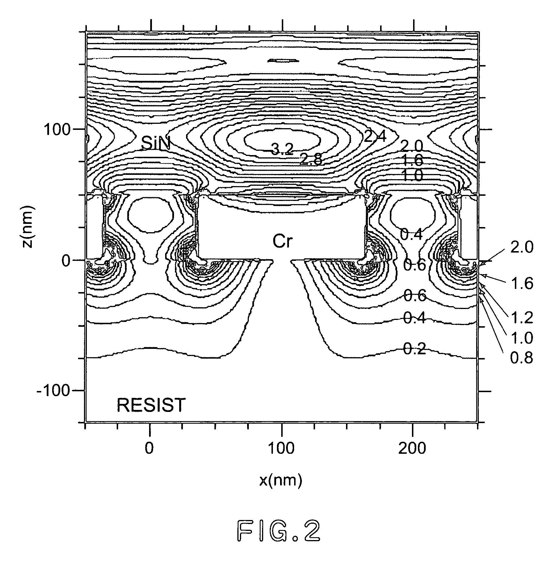
[0030]FIG. 4 shows an example of the first mask used in an embodiment of the mask manufacturing method of the present invention. In the following description, as shown in FIG. 4, a width of each opening is referred to as an “opening width”, and a width of a light blocking film (a spacing between adjacent openings) is referred to as an “opening spacing”.

[0031] The first mask has an opening width which is smaller than a wavelength of exposure light described later. When light enters an opening having the opening width smaller than the light wavelength, it is possible to create a near field only in the vicinity of the opening.

[0032] In a f...


PUM


Abstract

A mask manufacturing method includes a first step of forming, on a workpiece substrate, a fine pattern on the basis of a pattern of a fine opening having a size of not more than a wavelength of exposure light by irradiating the workpiece substrate with the exposure light through a first mask provided with the fine opening and using near-field light leaking from the fine opening; and a second step of forming a second mask by processing the workpiece substrate on the basis of the fine pattern formed in the first step.

Description

FIELD OF THE INVENTION AND RELATED ART [0001] The present invention relates to a mask manufacturing method using lithography permitting formation of a fine pattern. [0002] Increasing capacity of a semiconductor memory and increasing speed and density of a CPU processor have inevitably necessitated further improvements in fineness of microprocessing through optical lithography. Generally, the limit of microprocessing with an optical lithographic apparatus is of an order of the wavelength of light used. Thus, the wavelength of light used in optical lithographic apparatuses has been shortened more and more. Currently, near ultraviolet laser is used, and microprocessing of 0.1 μm order is enabled. While the fineness is being improved in the optical lithography, in order to assure microprocessing of 0.1 μm or narrower, there still remain many unsolved problems such as further shortening of wavelength of laser light, development of lenses usable in such wavelength region, and the like. [0...

Claims


Application Information

Patent Timeline
IPC IPC(8): G03C5/00G03F1/24G03F1/68G03F7/20G03F9/00H01L21/027
CPCB82Y10/00G03F7/7035G03F1/14G03F1/50
Inventor YAMAGUCHI, TAKAKOINAO, YASUHISA
Owner CANON KK
Why Eureka
Try Eureka