Method and system for forming a mask pattern, method of manufacturing a semiconductor device, system forming a mask pattern on data, cell library and method of forming a photomask

a cell library and mask pattern technology, applied in the field of mask pattern, can solve the problems of large chip area, increased photomask area, and inability to secure desired dimensional accuracy at the boundary portion of cell pattern,

Inactive Publication Date: 2005-03-24
KK TOSHIBA
View PDF11 Cites 23 Cited by
  • Summary
  • Abstract
  • Description
  • Claims
  • Application Information

AI Technical Summary

Problems solved by technology

However, the prior arts described above have the problem when the cell patterns subjected to the PPC are placed on a chip.
As a result, desired dimensional accuracy is not secured at the boundary portion between cell patterns.
However, if the methods are applied to all cell patterns, the area of the photomask increases, leading larger chip area.

Method used


Image

  • Method and system for forming a mask pattern, method of manufacturing a semiconductor device, system forming a mask pattern on data, cell library and method of forming a photomask
  • Method and system for forming a mask pattern, method of manufacturing a semiconductor device, system forming a mask pattern on data, cell library and method of forming a photomask
  • Method and system for forming a mask pattern, method of manufacturing a semiconductor device, system forming a mask pattern on data, cell library and method of forming a photomask

Examples


first embodiment

[0025] (First Embodiment)

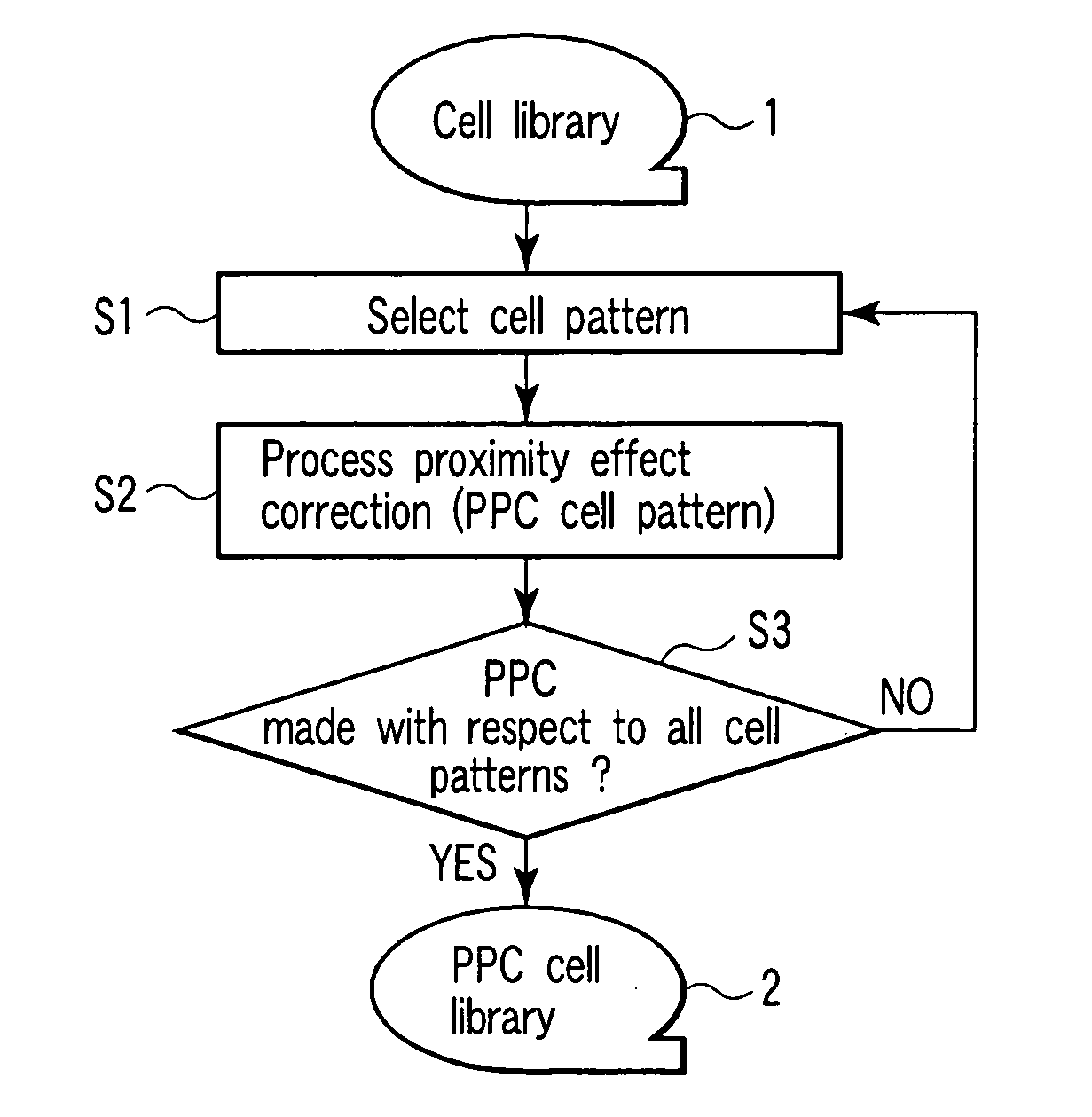
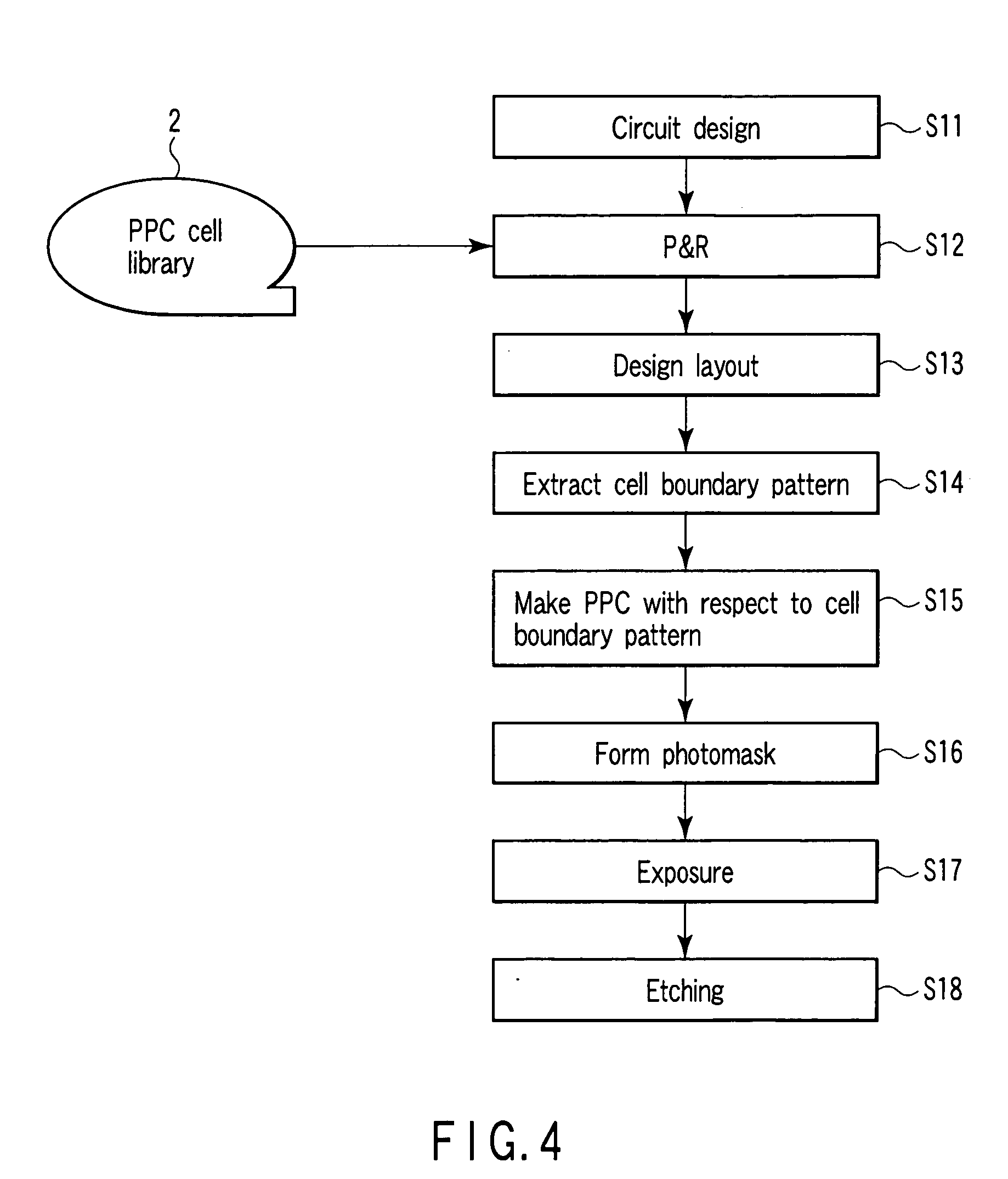
[0026] As referred to the cell library in the background technique, the procedure of making PPC with respect to cell patterns included in the cell library to prepare a new cell library on data will firstly be explained below. FIG. 1 is a flowchart to explain the method of preparing a new cell library having cell patterns by executing PPC to cell patterns in a cell library. As shown in FIG. 1, a first cell pattern is selected from a cell library 1 (first cell library)(step S1). The cell library 1 stores cell patterns. The cell patterns are each composed of several patterns for realizing individual circuit characteristics (e.g., NAND gates and OR gates, etc.).

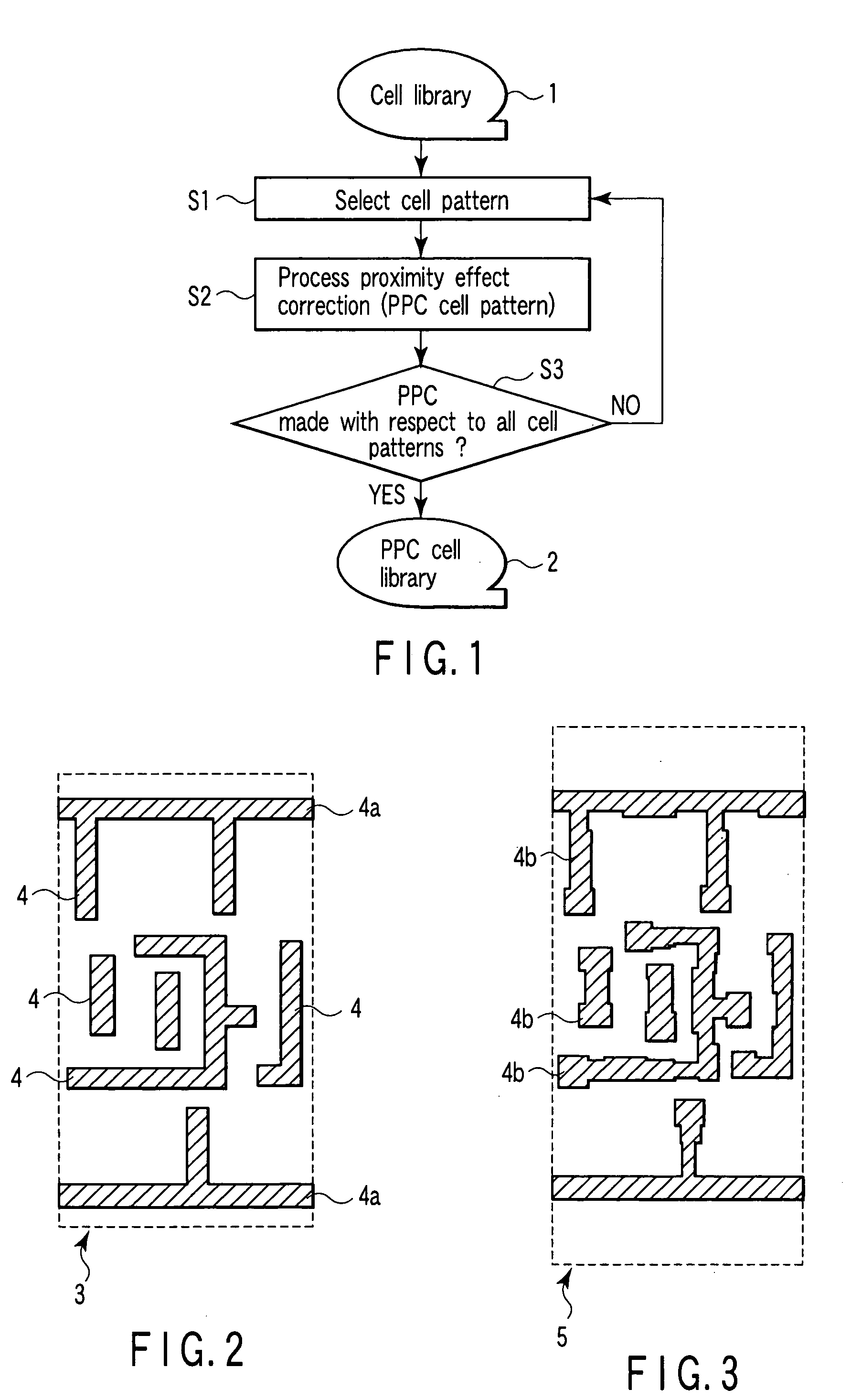
[0027] In FIG. 2, there is shown a cell pattern 3 of a metal interconnection layer as one example of the cell pattern. As illustrated in FIG. 2, the cell pattern 3 has several patterns 4. Typically, the cell pattern 3 of the metal interconnection layer has power line patterns 4a, which horizontally exten...

second embodiment

[0040] (Second Embodiment)

[0041] In the first embodiment, the PPC is made with respect to the cell pattern 3 of the cell library 1 itself to prepare the PPC cell library 2. In the second embodiment, the PPC is made to the cell pattern 3 of the cell library 1 having an additional pattern placed in its neighborhood.

[0042]FIG. 5 schematically shows the configuration of a mask pattern forming system 11 according to the second embodiment. As shown in FIG. 5, the mask pattern forming system 11 has a pattern select section 12. The pattern select section 12 selects one cell pattern 3 from the cell library 1, and outputs the data of the selected cell pattern. The data from the pattern select section 12 is supplied to a dummy pattern generation section 13. The dummy pattern generation section 13 prepares data of a provisional cell pattern having a dummy pattern placed on both neighborhoods of the cell pattern 3 based on the method described later.

[0043] A first mask data process section 14 ...


PUM

PropertyMeasurementUnit
shapeaaaaaaaaaa
distanceaaaaaaaaaa
widthaaaaaaaaaa

Abstract

A method of forming a mask pattern comprises the following steps. A second cell library is prepared by making process proximity effect correction with respect to cell patterns stored in a first cell library. The second cell library stores corrected cell patterns. A first corrected cell pattern and a second corrected cell pattern of the corrected cell patterns are placed so that an edge of the first corrected cell pattern and an edge of the second corrected cell pattern contact or come close to or overlap each other. A boundary pattern at the boundary neighborhood between the first corrected cell pattern and the second corrected cell pattern is extracted. Process proximity effect correction is made with respect to the boundary pattern.

Description

CROSS-REFERENCE TO RELATED APPLICATIONS [0001] This application is based upon and claims the benefit of priority from prior Japanese Patent Application No. 2003-312745, filed Sep. 4, 2003, the entire contents of which are incorporated herein by reference. BACKGROUND OF THE INVENTION [0002] 1. Field of the Invention [0003] The present invention relates to a method of forming a mask pattern, a method of manufacturing a semiconductor device, a system forming a mask pattern on data, a cell library and a method of forming a photomask. Specifically, the present invention relates to a mask pattern for forming a photomask used for logic devices (application specific integrated circuits [ASICs], in particular). [0004] 2. Description of the Related Art [0005]FIG. 11 shows the flow after the layout design of a logic device such as an ASIC. Circuit design (step S31) is completed, and thereafter, a photomask having a pattern for realizing the designed circuit is formed. More specifically, cell p...

Claims


Application Information

Patent Timeline
Patent Type & Authority Applications(United States)
IPC IPC(8): G03F1/36G03F1/68G03F1/70G06F17/50H01J37/302H01L21/027
CPCG03F1/144H01J2237/31769H01J37/3026G03F1/36
Inventor KOTANI, TOSHIYATANAKA, SATOSHIINOUE, SHOICHI
Owner KK TOSHIBA
Why Eureka
Try Eureka