Method for correcting mask distribution pattern

A technology of layout drawing and mask, applied in photoengraving process of pattern surface, original for photomechanical processing, special data processing application, etc., can solve problems such as low pattern density and uneven etching, and achieve improved surface The effect of uniformity and improving product yield

Inactive Publication Date: 2003-10-22
UNITED MICROELECTRONICS CORP
View PDF0 Cites 20 Cited by
  • Summary
  • Abstract
  • Description
  • Claims
  • Application Information

AI Technical Summary

Problems solved by technology

like figure 2 As shown, the etched line width w' of each element pattern on the mask layout diagram may be affected by microload or other system error factors, resulting in uneven etching. For example, the etched line width of each element pattern may vary with the line width The distance increases and increases, that is to say, the lower the pattern density, the more isolated linear pattern may obtain a larger line width after etching than the denser linear pattern.

Method used


Image

  • Method for correcting mask distribution pattern
  • Method for correcting mask distribution pattern
  • Method for correcting mask distribution pattern

Examples


Embodiment Construction

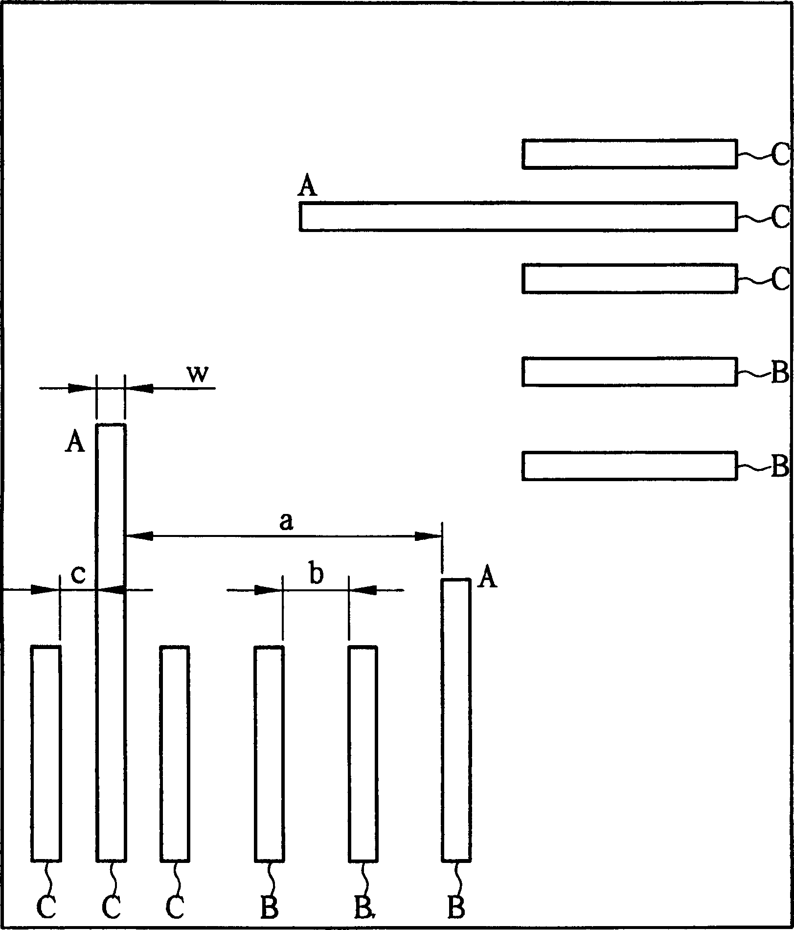
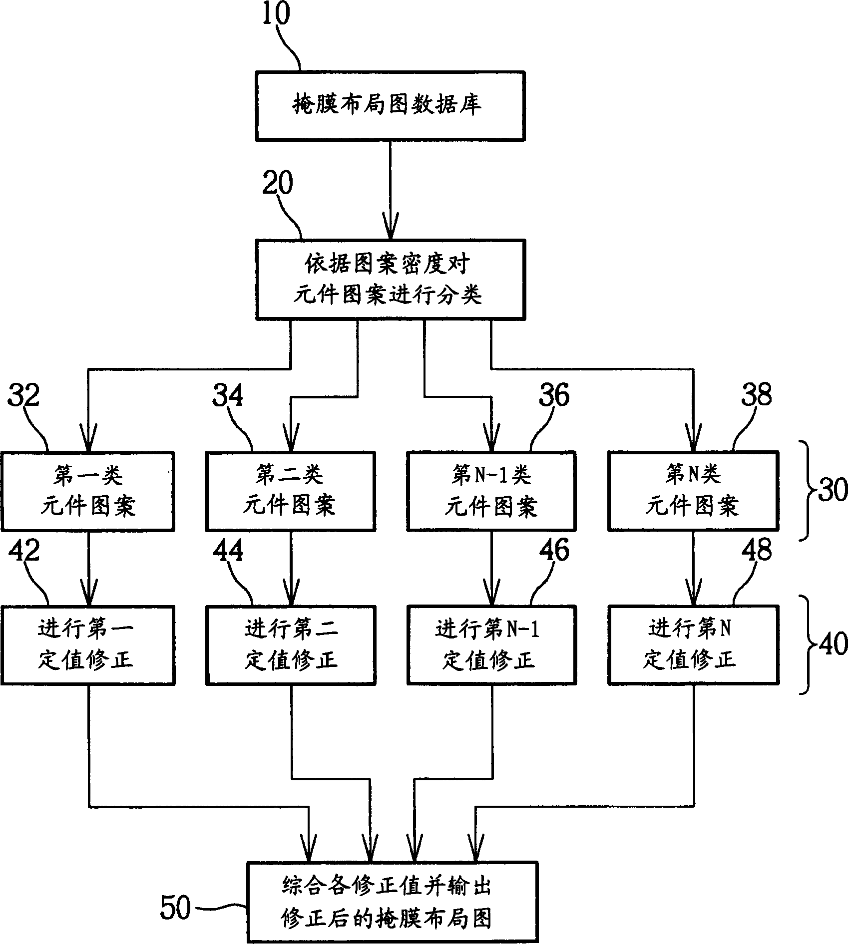
[0022] refer to image 3 , image 3 A flowchart of a method for correcting a mask layout to avoid microloading effects according to the present invention. Such as image 3 As shown, the method of the present invention first proceeds to step 10, providing a mask layout database. The mask layout diagram contains a plurality of (linear) element patterns, which are respectively used to define conductive regions in different regions on a single chip, such as word lines or bit lines in memory cell regions and logic circuit regions, etc. Component patterns for different circuit design requirements, or used to define component patterns on a multi-chip, and the database includes parameter data of each component pattern.

[0023] Since the micro-loading effect is caused by the pattern density difference between the various element patterns, the present invention then proceeds to step 20, provides a detection program, and classifies according to the pattern density of each element pat...


PUM


Abstract

The invention provides a method to correct the mask layout, the layout including multiple cell patterns with different densities. It firstly carries out a detecting program, and according to the densities separates various component patterns into multiple kinds of cell patterns, and finally corrects various kinds of cell patterns, respectively.

Description

technical field [0001] The invention provides a method for correcting a mask layout, in particular a method for correcting a systematic error generated when a mask layout is transferred in a pattern. Background technique [0002] In order to form a designed integrated circuit (IC) on a semiconductor chip, a semiconductor foundry (semiconductor foundry) must first make a mask (mask), and form a designed layout (layout) pattern on the mask, and then The photolithography process transfers the pattern on the mask to the photoresist on the semiconductor chip at a certain ratio after exposure and development, and then uses the etching process to remove the area not covered by the photoresist on the semiconductor chip. Substances on the surface, such as silicon or silicon dioxide, are removed. Therefore, the pattern on the mask is first transferred to the photoresist and then to the semiconductor chip through two processes of photolithography and etching. T...

Claims


Application Information

Patent Timeline
Patent Type & Authority Applications(China)
IPC IPC(8): G03F1/72G03F7/00G06F17/00
Inventor 李启明范政文黄俊仁刘智强
Owner UNITED MICROELECTRONICS CORP
Why Eureka
Try Eureka