Interdigital capacitor and method for adjusting the same

a digital capacitor and digital capacitor technology, applied in the field of devices having capacitors, can solve the problems of affecting the circuit operation, the oscillator employing the mim capacitor will have a frequency error, and the current technology has a difficulty in accurate electrode production

Inactive Publication Date: 2005-03-24
FUJITSU QUANTUM DEVICES LTD
View PDF8 Cites 10 Cited by
  • Summary
  • Abstract
  • Description
  • Claims
  • Application Information

AI Technical Summary

Benefits of technology

[0014] A general object of the present invention is to provide an interdigital capacitor and a method for adjusting the same in which the above disadvantages are eliminated.

Problems solved by technology

Such a deviation of the capacitance will affect the circuit operation.
For example, the oscillator employing the MIM capacitor will have a frequency error that depends on a capacitance deviation.
It is to be noted that current technology has a difficulty in accurate production of an electrode pattern of MIM capacitor having a side equal to or smaller than 10 μm.
However, the above-mentioned two conventional techniques cannot be used in the millimeter wave band over 30 GHz.
However, it is impossible to accurately adjust the capacitance as small as 0.05 pF used in the millimeter wave band equal to or higher than 30 GHz (for example, by the 0.005 pF step).
The adjustment method proposed in Japanese Unexamined Patent Publication No. 8-130433 has a problem arising from forming the oxide film.
If an element exists in the vicinity of the interdigital capacitor, the element may be damaged at the time of forming the oxide film by anode oxidization.
Thus, the method cannot be suitably applied to MMIC in which the interdigital capacitor is required to be arranged close to an FET (Field Effect Transistor) or the like.
Besides the above, there is another disadvantage in which a parasitic capacitor is connected to a pad necessary for anode oxidization.

Method used


Image

  • Interdigital capacitor and method for adjusting the same
  • Interdigital capacitor and method for adjusting the same
  • Interdigital capacitor and method for adjusting the same

Examples


second embodiment

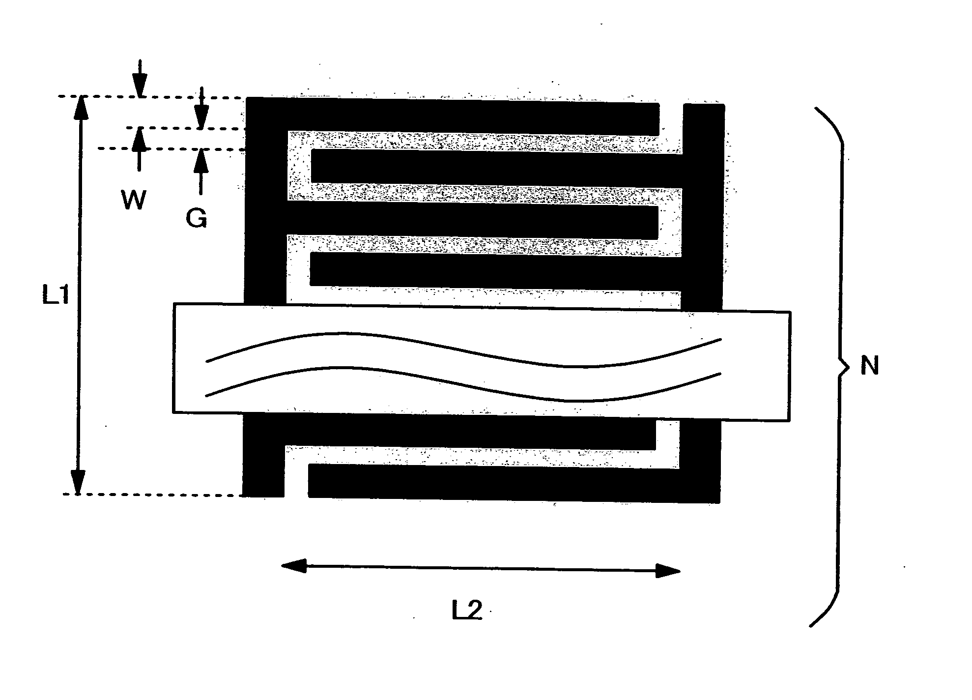
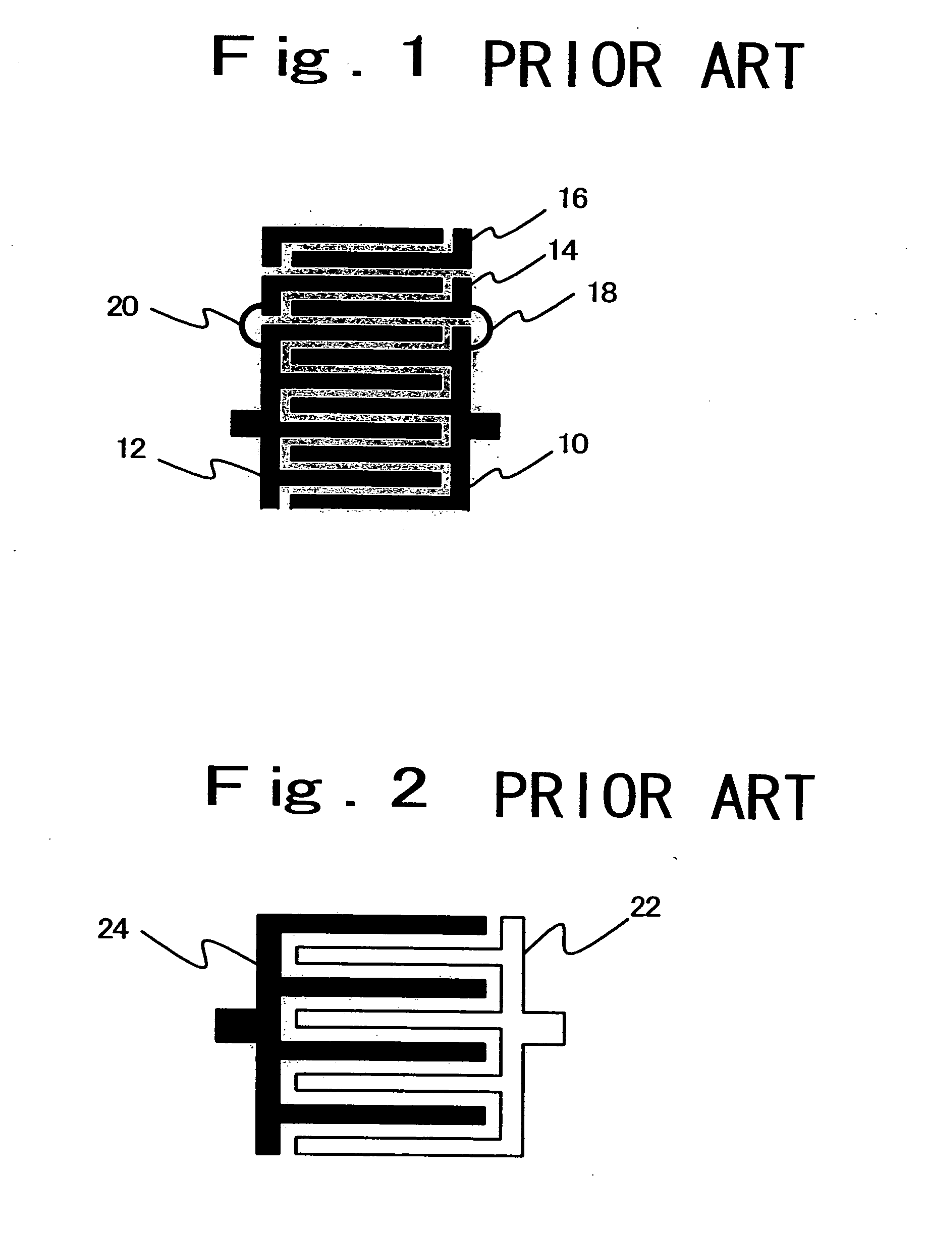
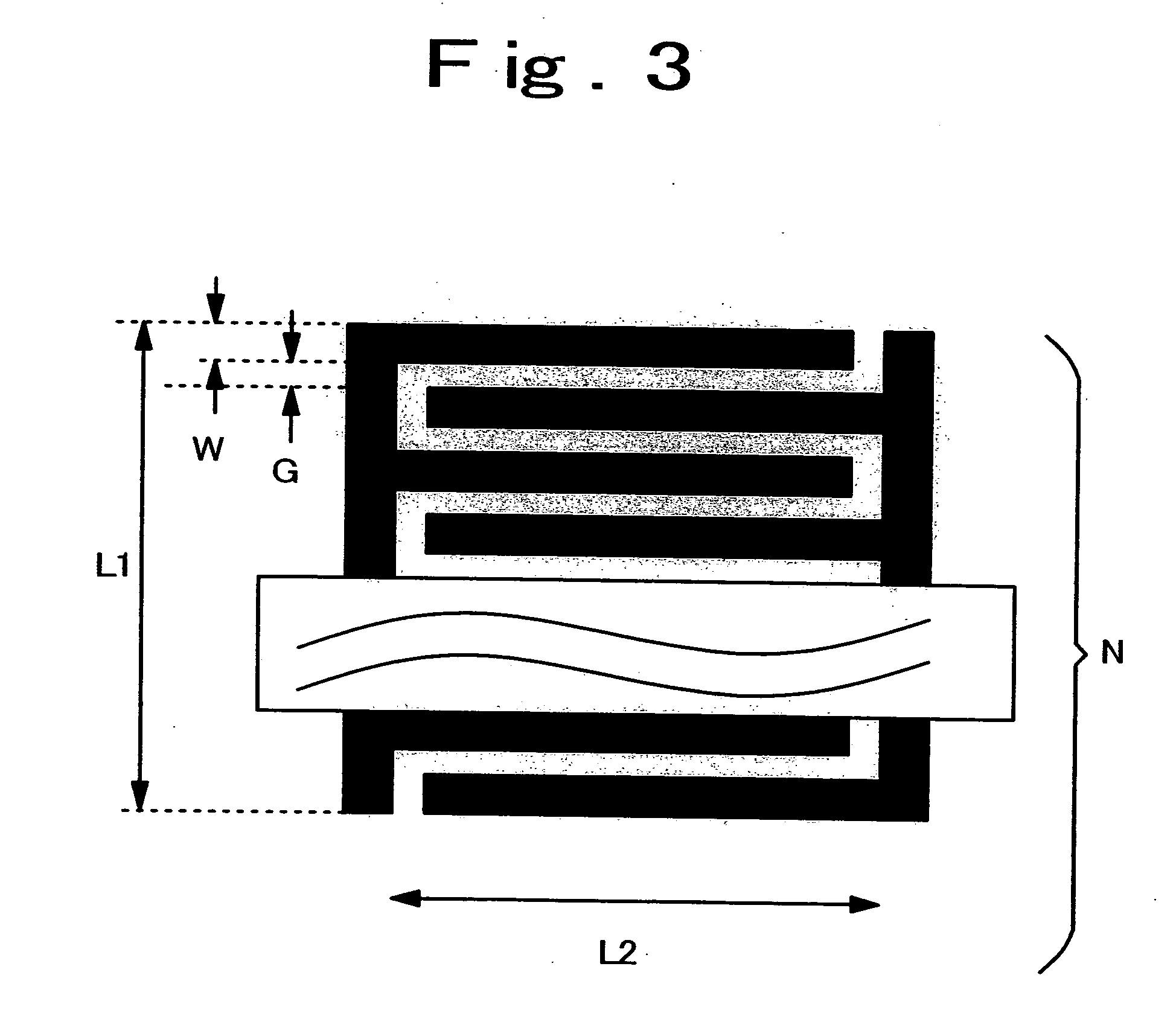
[0052]FIG. 5 is a plan view of an interdigital capacitor according to a second embodiment of the present invention. This interdigital capacitor has comb-like electrodes 40 and 41 that are paired and formed on a semiconductor substrate made of, for example, silicon or semi-insulating GaAs. The bus lines of the comb-like electrodes 40 and 41 have comparatively narrow portions 42 and 43. The narrow portions 42 and 43 are narrower than the remaining portions of the comb-like electrodes 40 and 41, and are subject to cutting for capacitance adjustment. The narrow portions 42 and 43 of the bus lines can be cut by relatively weak laser energy. The narrow portions 42 and 43 may be defined as cutting targets. The narrowed cutting targets contribute to reducing the amount of metal scattered at the time of cutting. In FIG. 5, the cutting targets 42 and 43 face each other. However, the cutting targets 42 and 43 may be arranged in another way. Only one of the cutting targets 42 and 43 may be prov...

third embodiment

[0053]FIG. 6 is a plan view of an interdigital capacitor according to a third embodiment of the present invention. Comb-like electrodes 46 and 47 formed on a semiconductor substrate have approximately C-shaped bus line portions 48 and 49, respectively. The portion 48 serves as a cutting target and is curved outward from the bus line. Similarly, the portion 49 serves as a cutting part and is curved outward from the bus line. No electrode fingers are formed to the bus line portions 48 and 49, which are dedicated to trimming. Each of the comb-like electrodes 46 and 47 may be divided into two parts by cutting the bus line portions 48 and 49 by laser. The cutting target portions 36 and 37 are away from the electrode fingers involved in making capacitance, so that the electrode fingers can be less affected due to cutting.

[0054] The approximately C-shaped bus line portions 48 and 49 may be narrowed like the second embodiment of the present invention. The third embodiment of the present in...

fourth embodiment

[0055]FIG. 7A is a plan view of an interdigital capacitor according to a fourth embodiment of the present invention, and FIG. 7B is a cross-sectional view taken along a line VIIB-VIIB shown in FIG. 7A. A bus lie 54 of a comb-like electrode 52 formed on a semiconductor substrate has a cutting target portion 56. Similarly, a bus line 55 of a comb-electrode 53 formed on the semiconductor substrate has a cutting target portion 57. The cutting target portions 56 and 57 may have an identical structure. FIG. 7B illustrates a cross section of the cutting target portion 56. The bus line 54 formed on the semiconductor substrate, now assigned a reference numeral 61, is divided into two portions. An area defined by the opposing ends of the divided portions is full of an insulating film 62, which also covers the entire surface of the semiconductor substrate 61. Vias 59 and 60 are provided in the insulating film 62. These vias 59 and 60 have via holes formed in the insulating film 62, which are f...


PUM


Abstract

An interdigital capacitor includes a semiconductor substrate, and a pair of comb-like electrodes formed on the semiconductor substrate. At least one of the pair of comb-like electrodes includes a cutting target portion.

Description

CROSS REFERENCE OF RELATED APPLICATIONS [0001] This application is a Divisional of application Ser. No. 10 / 396,502, which was filed on Mar. 26, 2003.BACKGROUND OF THE INVENTION [0002] 1. Field of the Invention [0003] The present invention generally relates to a device having a capacitor, such as an oscillator, and more particularly, to an interdigital capacitor used in a high-frequency circuit and a method for adjusting the same. [0004] 2. Description of the Related Art [0005] An MIM (Metal Insulator Metal) capacitor and an interdigital capacitor are known as capacitors used in high-frequency circuits that handle a frequency as high as 1 GHz or over. Usually, these capacitors are incorporated in an MMIC (Monolithic Microwave Integrated Circuit). For example, the MIM is made up of a pair of electrodes formed on a semi-insulating GaAs substrate, and a dielectric member sandwiched between the pair of electrodes. The interdigital capacitor has an interdigital electrode pattern formed on...

Claims


Application Information

Patent Timeline
Patent Type & Authority Applications(United States)
IPC IPC(8): H01G4/255H01L21/822H01L23/522H01L27/04H01L27/08H03H3/10H03H9/145
CPCH01L23/5223H01L27/0805H01L2924/0002H01L2924/00
Inventor MIYAZAWA, NAOYUKI
Owner FUJITSU QUANTUM DEVICES LTD
Why Eureka
Try Eureka