

Method of controlling critical dimension microloading of photoresist trimming process by selective sidewall polymer deposition
- Summary
- Abstract
- Description
- Claims
- Application Information
AI Technical Summary
Benefits of technology
Problems solved by technology
Method used
Image

Examples
Embodiment Construction
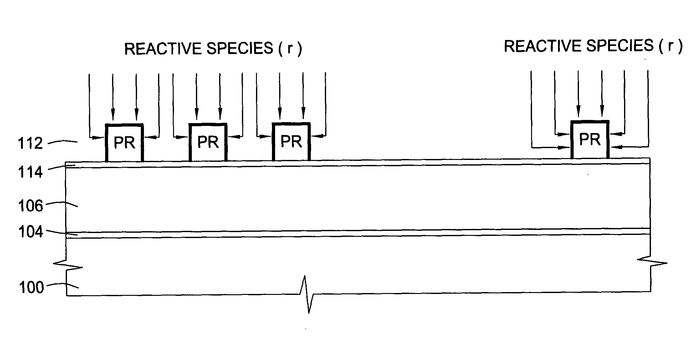
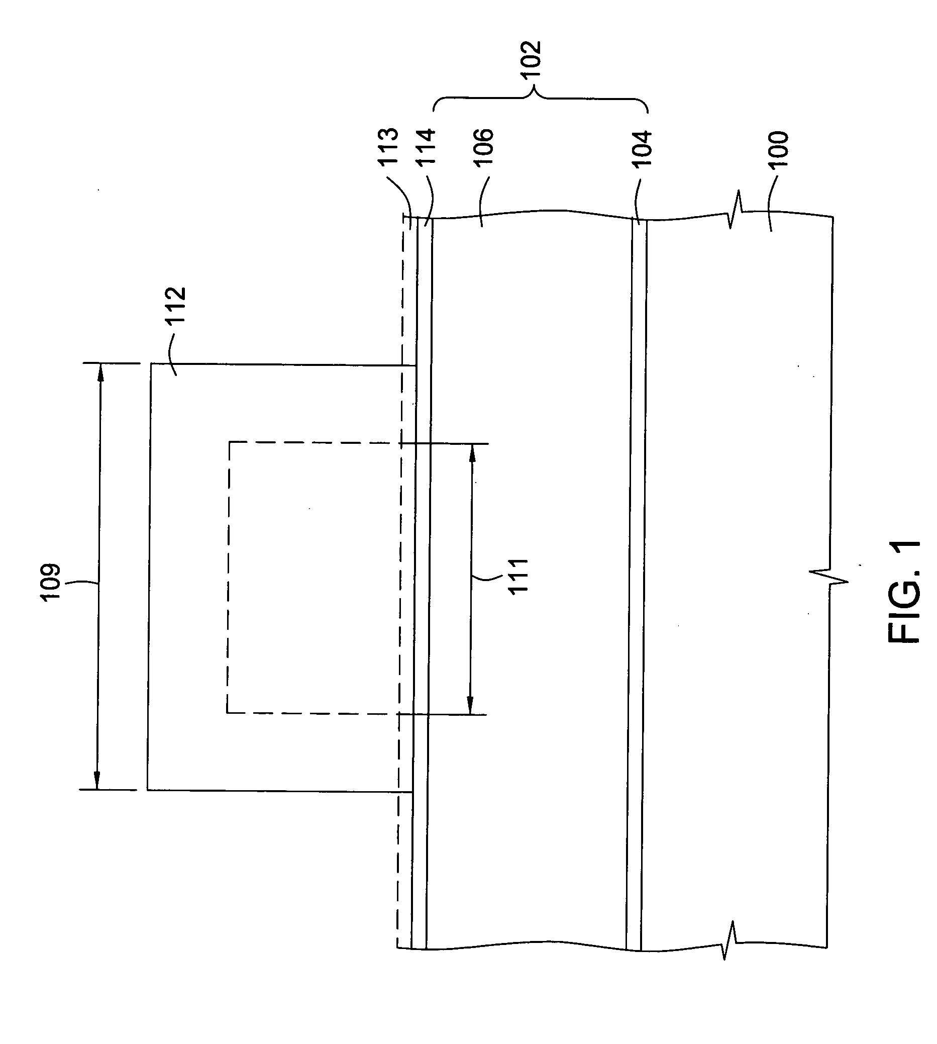
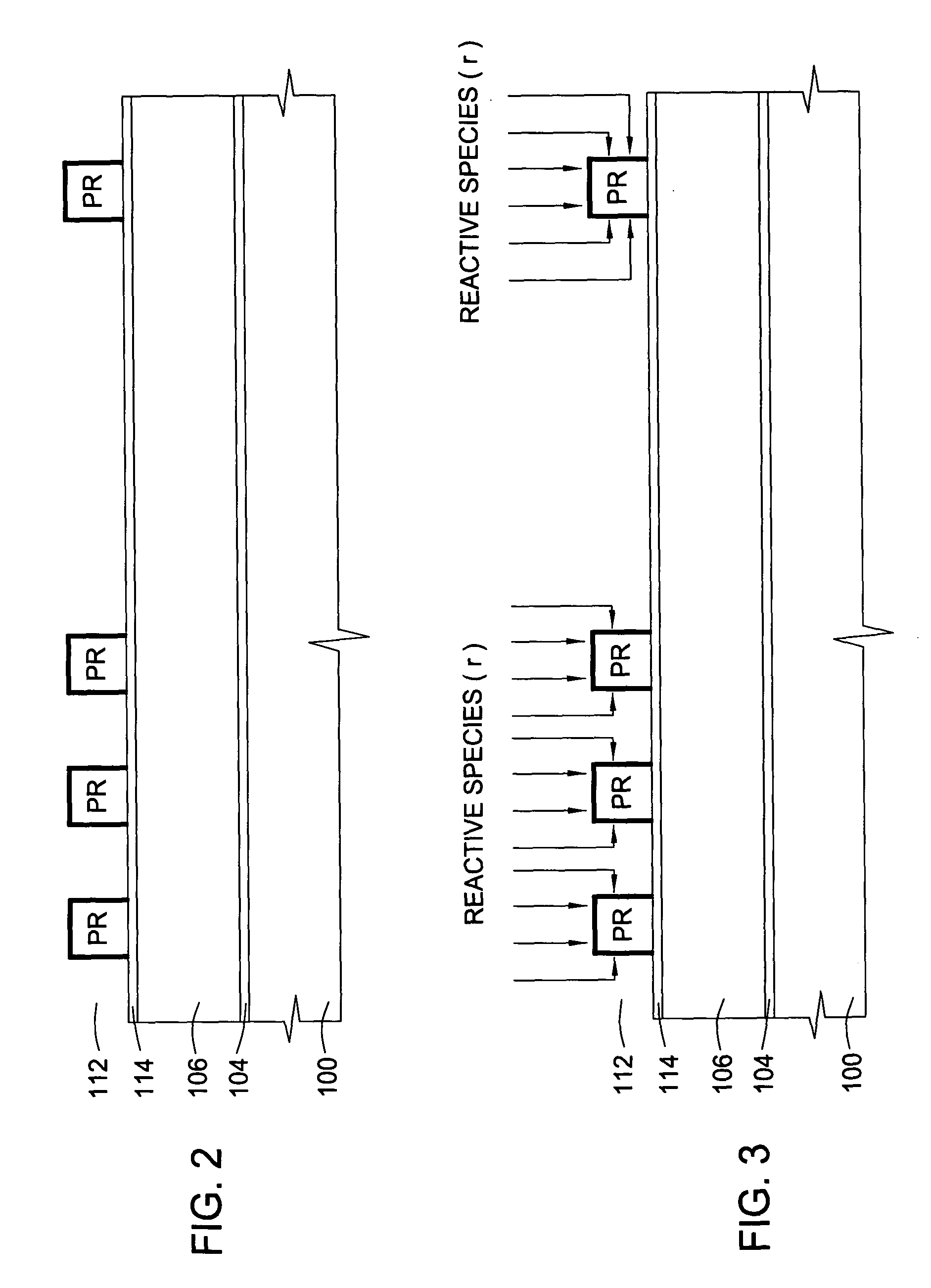
[0020]FIG. 1 illustrates a cross-sectional view of a portion of a composite structure having a photoresist mask thereon prior to trimming. The composite structure comprises a substrate 100, upon which is a film stack 102, within which a structure, e.g., a gate, is to be formed thereon. The film stack 102 generally comprises a gate electrode layer 106 and a gate dielectric layer 104. The gate electrode is patterned by a photoresist mask 112 (e.g. photoresist patterned mask), an optional film of an anti-reflective coating (ARC) 113 (shown only in FIG. 1 with dashed lines), as well as a hard mask 114, underneath.
[0021] The hard mask 114 is generally used as an etch mask for etching both the gate electrode layer 106 and the gate dielectric layer 104 and may comprise, for example, silicon dioxide (SiO2), silicon oxynitride (SiON), amorphous carbon (i.e., α-carbon), Advanced Patterning Film™ (APF) (available from Applied Materials, Inc. of Santa Clara, Calif.), and the like.
[0022] In on...
PUM
 Abstract
Description
Claims
Application Information