Diffractive imaging spectrometer

a diffractive imaging and spectrometer technology, applied in the field of spectral devices, can solve the problems of low resolution of small-scale spectrometers and unacceptably large devices, and achieve the effects of wider spectral range, improved resolution and small siz

Active Publication Date: 2005-03-31
WAYNE STATE UNIV
View PDF3 Cites 44 Cited by
  • Summary
  • Abstract
  • Description
  • Claims
  • Application Information

AI Technical Summary

Benefits of technology

[0024] In a specific illustrative embodiment of the invention, a DIS has a footprint less than 2×1 mm2, is about 2.5 mm tall (excluding the image sensor, which in may be a CCD matrix), covers the entire visible spectral range from 400 nm to 700 nm with resolution of approximately from 2 nm to 4 nm ac

Problems solved by technology

Unfortunately, small footprint spectrometers have low resolution.
However, these devices still

Method used


Image

  • Diffractive imaging spectrometer
  • Diffractive imaging spectrometer
  • Diffractive imaging spectrometer

Examples


Embodiment Construction

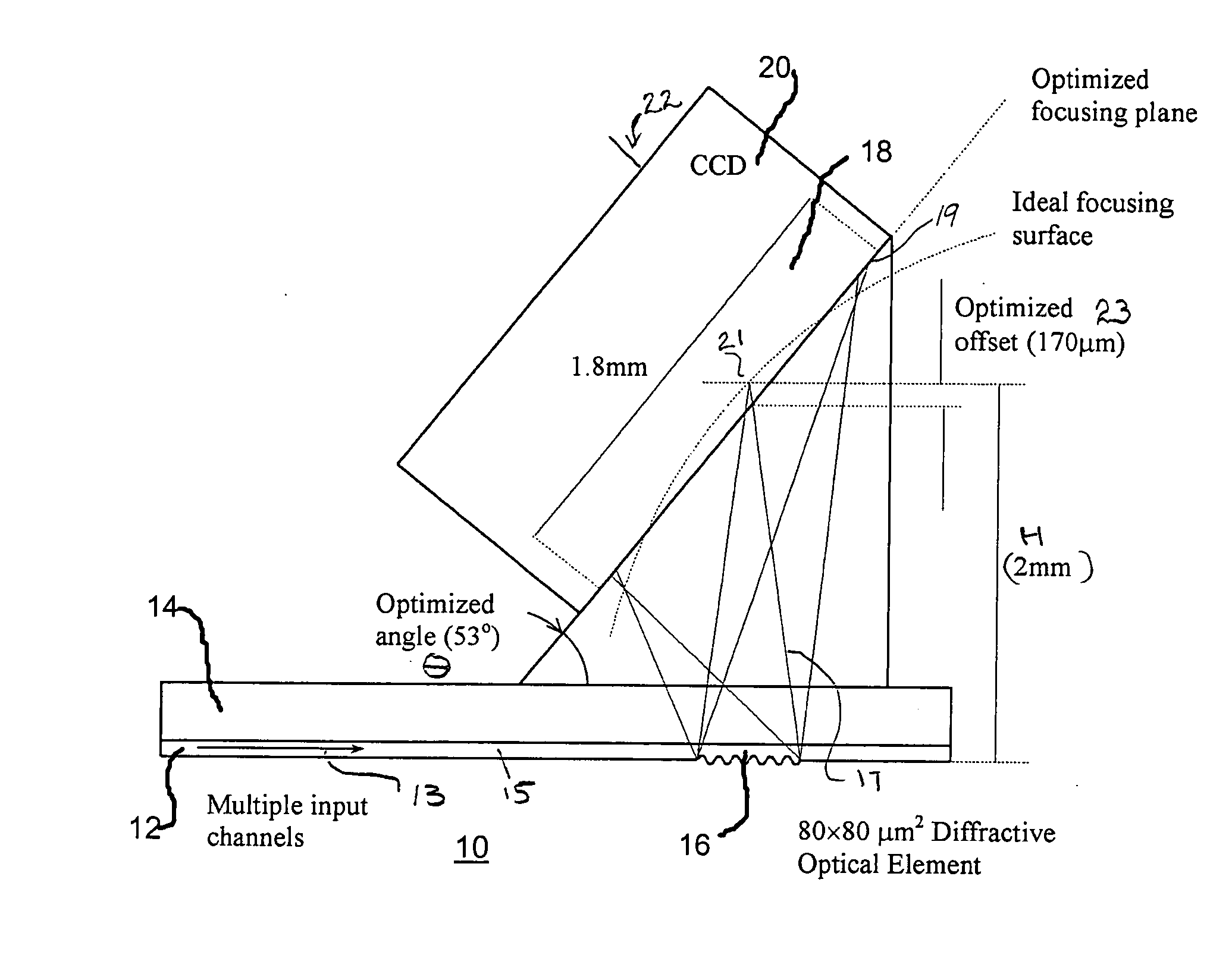
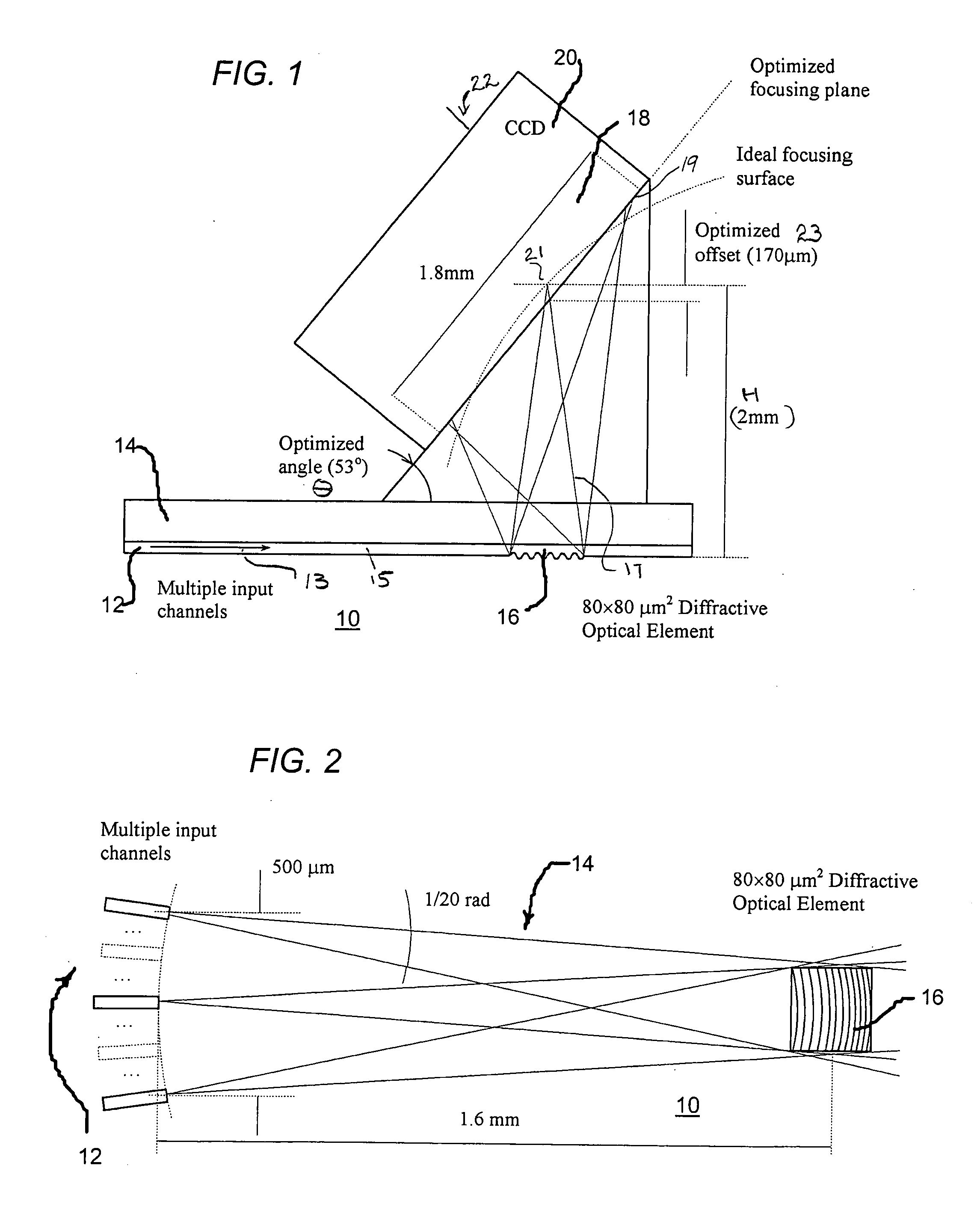
[0032]FIG. 1 is a simplified schematic representation of a side view of DIS 10 constructed in accordance with the principles of the invention. As shown in this figure, DIS 10 has N input waveguide channels 12, a planar waveguide expansion section 14, a diffractive optical element 16, an aberration correction prism 18, and an image sensor 20. In this particular embodiment, the image sensor is illustratively a Charge Coupled Device (CCD).

[0033] The input optical signals 13 travel through waveguide channels 12 in planar waveguide 15 that also contains diffractive optical element 16. Diffractive optical element 16 produces focused output signals 17 that impinge on a focusing surface 19 on aberration correction prism 18 to produce an output image 21 responsive to the focused output signal. The image sensor 20, illustratively a CCD which is an array of photodetectors, or inputs, not specifically shown in this figure, receives the output image(s) and produces at an output 22, an image ele...


PUM


Abstract

A miniaturized diffractive imaging spectrometer (DIS) has a footprint less than 2×1 mm2, is about 2.5 mm tall (excluding an image detector, which in some embodiments may be a CCD matrix), and covers the entire visible spectral range from 400 nm to 700 nm with resolution of approximately from 2 nm to 4 nm across the field. The DIS is able to function with multiple input waveguide channels, and is flexible in its various possible configurations, as it can be designed to achieve better resolution or higher number of channels or wider spectral range or smaller size.

Description

RELATIONSHIP TO OTHER APPLICATION(S) [0001] This application claims the benefit under 35 U.S.C. § 119 of provisional application 60 / 473,958 filed on Mar. 27, 2003.BACKGROUND OF THE INVENTION [0002] 1. Field of the Invention [0003] This invention relates generally to spectral devices for applications such as lab-on-a-chip for biological and chemical analysis, and more particularly, to a Diffractive Imaging Spectrometer (“DIS”) in the form of a highly compact device, which takes multiple optical input signals from input channel waveguides, and produces a spectrally resolved image, covering a wide spectral range with high resolution. [0004] 2. Description of the Related Art [0005] Small scale spectral devices are required for applications, such as lab-on-a-chip, for biological and chemical analysis. The integration of microfluidics, microelectronics, and integrated optics on a single chip or wafer is essential for the practical implementation of a micro total analysis system (μTAS), fo...

Claims


Application Information

Patent Timeline
IPC IPC(8): G01J3/18G01J3/28
CPCG01J3/0205G01J3/0259G01J3/2823G01J3/18G01J3/0294
Inventor AVRUTSKY, IVAN
Owner WAYNE STATE UNIV
Why Eureka
Try Eureka