Semiconductor memory

a technology of semiconductors and memory, applied in the field of semiconductor memory, can solve problems such as increased leak current, deterioration in reading-out speed, and increase in the amount of leak current, so as to improve the performance of cache access

Inactive Publication Date: 2005-03-31
PANASONIC CORP
View PDF3 Cites 34 Cited by
  • Summary
  • Abstract
  • Description
  • Claims
  • Application Information

AI Technical Summary

Benefits of technology

[0042] The special bit is a hit signal. In this case, the transistor substrate potential of the cache memory cell can be varied at the time of hit and the time of mishit of the cache. Thereby, the performance of the cache access can be improved.
[0043] Also,...

Problems solved by technology

For a transistor of the memory cell, the one with a short gate width is used, which raises the issues of deterioration in the reading-out speed and an increase in the amount of a leak current.
However, a static noise margin (simply referred to as noise margin hereinafter), which is an index of stability of the memory ...

Method used


Image

  • Semiconductor memory
  • Semiconductor memory
  • Semiconductor memory

Examples


first embodiment

[0059] (First Embodiment)

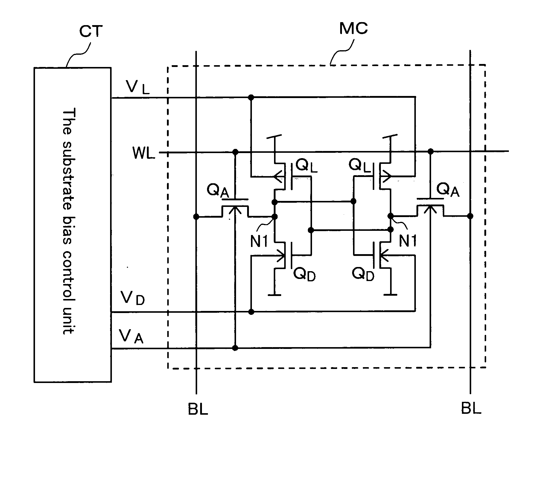
[0060] As shown in FIG. 1, a semiconductor memory according to a first embodiment comprises a static-type memory cell MC and a substrate bias control unit CT for applying bias onto a transistor substrate of the memory cell MC.

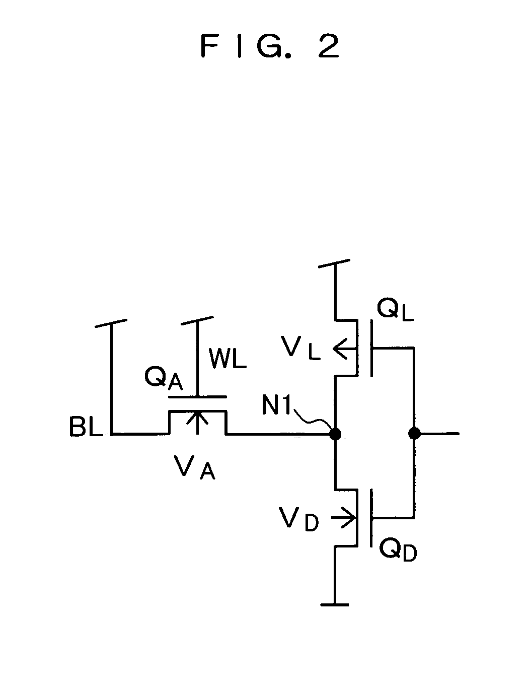
[0061] The memory cell MC is configured with a pair of access transistors QA formed with NMOS transistors, a pair of drive transistors QD formed with NMOS transistors, and a pair of load transistors QL formed with PMOS transistors. The pair of load transistors QL and the pair of drive transistors QD form a memory storage. The junction point between the load transistor QL and the drive transistor QD is a memory storage node N1 to which the access transistors QA is connected.

[0062] The substrate bias control unit CT increases the access speed at the time of making access to the memory cell MC by adjusting electric current flown to the memory storage node N1 of the memory cell MC. In the meantime, it applies bias for improving the stabil...

second embodiment

[0088] (Second Embodiment)

[0089] A semiconductor memory according to a second embodiment of the present invention will be described by referring to FIG. 4. Shown in the illustration is an example of a SRAM memory cell array with four columns, four rows, and 1 bit output. In FIG. 4, reference numerals C1, C2, C3, C4 are the columns. Reference numerals W1, W2, W3, W4 are word lines being connected to the gates of the access transistor QA of each column. Reference numeral BL is a bit line being connected to the drains of the access transistors Q of each row. Reference numerals VLa1, VLa2, VLa3, VLa4 are the substrate potentials of the load transistors QL of each column, VDa1, VDa2, VDa3, VDa4 are the substrate potentials of the drive transistors QD of each column, and VAa1, VAa2, VAa3, VAa4 are the substrate potentials of the access transistors QA of each column. The same substrate potential is applied to the transistors of the memory cell in the same column. The substrate potential is...

third embodiment

[0096] (Third Embodiment)

[0097] A semiconductor according to a third embodiment of the present invention will be described by referring to FIG. 5. In FIG. 5, the same reference numerals as those of the second embodiment in FIG. 2 denote the same structural elements so that detailed description is omitted. Reference numerals L1, L2, L3, L4 are rows. Reference numerals VLb1, VLb2, VLb3, VLb4 are the substrate potentials of the load transistors QL, VDb1, VDb2, VDb3, VDb4 are the substrate potentials of the drive transistors QD, and VAb1, VAb2, VAb3, VAb4 are the substrate potentials of the access transistors QA. The same substrate potentials are applied to the transistors of the memory cell in the same column. The substrate potentials are separately applied to the transistors of the memory cell in different columns. Reference numerals CT21, CT22, CT23, CT24 are the substrate bias control units of each column.

[0098] With this configuration, it is possible to apply separate substrate po...


PUM


Abstract

A semiconductor memory of the present invention comprises: a static-type memory cell constituted of a pair of access transistors formed with NMOS transistors, a pair of drive transistors formed with NMOS transistors, and a pair of load transistors formed with PMOS transistors. Further, it comprises a substrate bias control unit which applies bias for increasing access speed to a substrate of any of the transistors when making access to the memory cell through adjusting electric current flown to a memory storage node in a common junction point of the three types of transistors. A substrate potential which is appropriate for reading-out, writing, memory-storing operation and low leak is applied.

Description

BACKGROUND OF THE INVENTION [0001] 1. Field of the Invention [0002] The present invention relates to a semiconductor memory having static-type memory cells. [0003] 2. Description of the Related Art [0004] Recently, the size of a SRAM memory cell has been remarkably reduced in size in accordance with processes which have become minuter. For a transistor of the memory cell, the one with a short gate width is used, which raises the issues of deterioration in the reading-out speed and an increase in the amount of a leak current. When using a transistor with low threshold voltage for achieving high-speed reading-out, the leak current is increased. On the contrary, when using a transistor with high threshold voltage for suppressing the leak current, memory cell current is decreased so that the speed of reading-out is decreased. [0005] In order to achieve both high-speed reading-out and low leak current, it is proposed to kinetically change substrate potential of a substrate of the memory ...

Claims


Application Information

Patent Timeline
IPC IPC(8): G11C5/14G11C11/413G11C11/41G11C11/417
CPCG11C11/417G11C5/146
Inventor HOUMURA, SHIGEOOKUYAMA, HIROAKIKANEHARA, HIDENARISUMITANI, NORIHIKO
Owner PANASONIC CORP
Why Eureka
Try Eureka