

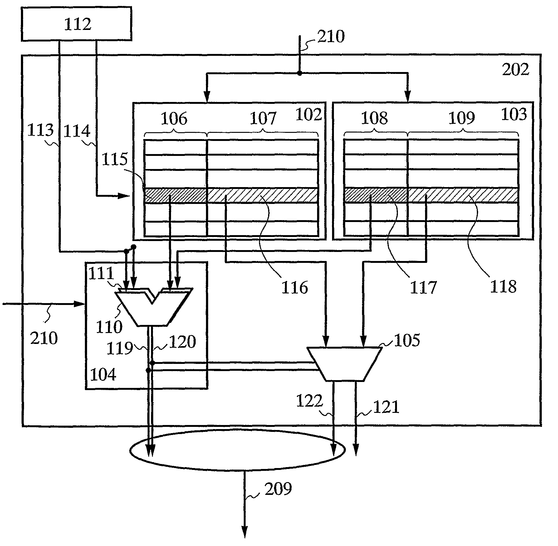
Selectively powering down tag or data memories in a cache based on overall cache hit rate and per set tag hit rate
a cache memory and cache technology, applied in the field of arithmetic processing devices, can solve the problems of ineffective read copy data, high power consumption of cache memory, and inability to read copy data, etc., to achieve faster processing of cpu, less cache misses, and increase cache memory capacity
- Summary
- Abstract
- Description
- Claims
- Application Information
AI Technical Summary
Benefits of technology
Problems solved by technology
Method used
Image

Examples
embodiment 1
[0064]In this embodiment, with respect to a CPU of the invention, on which a cache memory is mounted, description is made on the algorithm for determining a state of each set from the cache hit rate, for which a specific description is omitted in the embodiment mode.
[0065]Description is made on an algorithm in this embodiment in accordance with a flow chart shown in FIG. 5. A cache hit rate for access of an a number of times, which is an arbitrary number, is counted (cache hit rate counting 501). After the cache hit rate and b % which is a requirement set in advance are compared (requirement determining 502) and an arbitrary set is transitioned from an operating state to a resting state (process for stopping a set 503) in accordance with the result, a cache hit rate in an arbitrary period is counted (cache hit rate counting 504) and set to c %. By comparing the cache hit rate c % with b % which is the requirement set in advance (requirement determining 505), whether a state is resto...
embodiment 2
[0077]In this embodiment, with respect to a CPU of the invention on which a cache memory is mounted, description is made on an algorithm which is different from the algorithm for determining a resting set from a cache hit rate of Embodiment 1.
[0078]Description is made on an algorithm of this embodiment with reference to a flowchart in FIG. 6. An appropriate time period of d second is counted (time counting 601), an arbitrary set is transitioned from an operating state to a resting state (process for stopping a set 602), and then a cache hit rate is counted (cache hit rate counting 603). The cache miss rate is compared with e % which is a requirement set in advance (requirement determining 604), and whether a state is restored to a state before the transition or not is determined in accordance with the result (process for restoring a set 605). The algorithm corresponds to investigating a cache memory size and effectiveness thereof regularly, and testing whether the cache hit rate can...
embodiment 3
[0087]In this embodiment, description is made on a personal computer as a system using a CPU of the invention.
[0088]FIG. 7 shows a configuration of a personal computer. In FIG. 7, a CPU 702, a north bridge (NB) 703, a south bridge (SB) 704, an SDRAM 705, and an image processing circuit 706 are mounted on a mother board 701. On the SB 704, a hard disc controller 707, a flexible disc cartridge controller 708, a mouse controller 709, and a keyboard controller 710 are mounted. The image processing circuit 706, the hard disc controller 707, the flexible disc cartridge controller 708, a mouse 714, and a keyboard 715 control a display 711, a hard disc 712, a flexible cartridge 713, the mouse controller 709, and the keyboard controller 710 respectively.
[0089]Here, the NB 703 is a semiconductor device in which controller circuits for a semiconductor device which transfers data to and from the CPU 702 at a high speed, such as the SDRAM 705 and the image processing circuit 706, are integrated....
PUM
 Abstract
Description
Claims
Application Information