Development method for integrated circuits, program storage medium for storing the development method for integrated circuits, and concurrent development system, development program, and development method of ASIC and programmable logic device

a technology of integrated circuits and development methods, applied in logic circuits using specific components, instruments, program control, etc., can solve the problems of double management of design data, increase in development costs due to redesign and reevaluation of functions, and short development period of programmable logic devices, so as to reduce the development period of asic

Inactive Publication Date: 2005-03-31
FUJITSU LTD
View PDF5 Cites 33 Cited by
  • Summary
  • Abstract
  • Description
  • Claims
  • Application Information

AI Technical Summary

Benefits of technology

[0023] According to the above aspect, a core (logic core) of the programmable logic device is allocated from the ASIC core (logic core), while maintaining connection between blocks. Therefore, if verification of the programmable logic device using the core (logic core) is performed, duplication of verification at least in the same configuration can be avoided in the ASIC. Thus, concurrent development of the ASIC and the programmable logic device can proceed efficiently.
[0050] Further, according to the present invention, to create a netlist for the FPGA and the ASIC, on the one hand, FPGA design information is created in which the same terminals in a first design and a second design are connected, and a buffer corresponding to the FPGA is inserted between the terminals, from the first design in which terminal information of the FPGA including the whole or a part of functional blocks of a plurality of functional blocks is described, and the second design in which the same terminal information as that of the FPGA described as a low-order layer of the first design is described, and on the other hand, ASIC design information is created in which the same terminals in a third design and a fourth design are connected, and a buffer corresponding to the ASIC is inserted between the terminals, from the third design in which terminal information of the ASIC including the functional blocks is described, and the fourth design in which the same terminal information as that of the ASIC described as a low-order layer of the third design is described. This is followed by replacing each of the second design and the fourth design by the circuit information created based on the connection information of the functional blocks included in each design. Consequently, efficient concurrent development of the ASIC and the programmable logic device becomes possible, thereby reducing the development period of the ASIC.

Problems solved by technology

This results in problems such as double management of design data due to redesign, prolonged development period and an increase in the development cost due to redesign and reevaluation of functions.
The ASIC has a feature of prolonged development period but low cost, and in contrast, the programmable logic device (FPGA) has a feature of short development period but high cost.
However, with the electronic equipment becoming high-function and complicated, implementation design for performing specification design, logic design, floor plan, logic synthesis, layout design, and timing verification requires long time and it becomes difficult to ensure the design quality.
Particularly, remake of the ASIC development not only extends the development period of electronic equipment, but also increases cost and a loss of market investment opportunity.
Therefore, a programmable logic device having a short development turn around time (TAT) and an easy-to-change design is used in many occasions, but the programmable logic device is expensive, and its downsizing is difficult.
However, even if verification is performed by prototyping of the programmable logic device with the assumption of forming the ASIC, there is a problem in the serial development from the programmable logic device to the ASIC in that it is difficult to shorten the entire development process.
Particularly, when a timing problem occurs in the implementation design at the time of developing the ASIC, there is the possibility that redesign of the programmable logic device must be performed again.
Consigning the design to outside the company, such as a semiconductor vendor, causes an increase in the cost as well as in human resources in the consignee.
Further, when redesign takes place exclusively in the ASIC due to a difference in the structure between the programmable logic device and the ASIC device, not only does debugging by the programmable logic device become meaningless, but also the development period is prolonged to thereby cause a cost increase.
In either case, it causes a loss of market investment opportunity.
However, specification design, logic design and verification are prolonged due to complicated functions of the electronic equipment and fast market movement, and hence it becomes difficult to shorten the development process.
Further, when the development is executed concurrently, human resources having the knowledge of ASIC development and a development tool are necessary, thereby causing a problem in that training about the development tool, which becomes complicated with the progress of the semiconductor technology, becomes necessary.

Method used


Image

  • Development method for integrated circuits, program storage medium for storing the development method for integrated circuits, and concurrent development system, development program, and development method of ASIC and programmable logic device
  • Development method for integrated circuits, program storage medium for storing the development method for integrated circuits, and concurrent development system, development program, and development method of ASIC and programmable logic device
  • Development method for integrated circuits, program storage medium for storing the development method for integrated circuits, and concurrent development system, development program, and development method of ASIC and programmable logic device

Examples


first embodiment

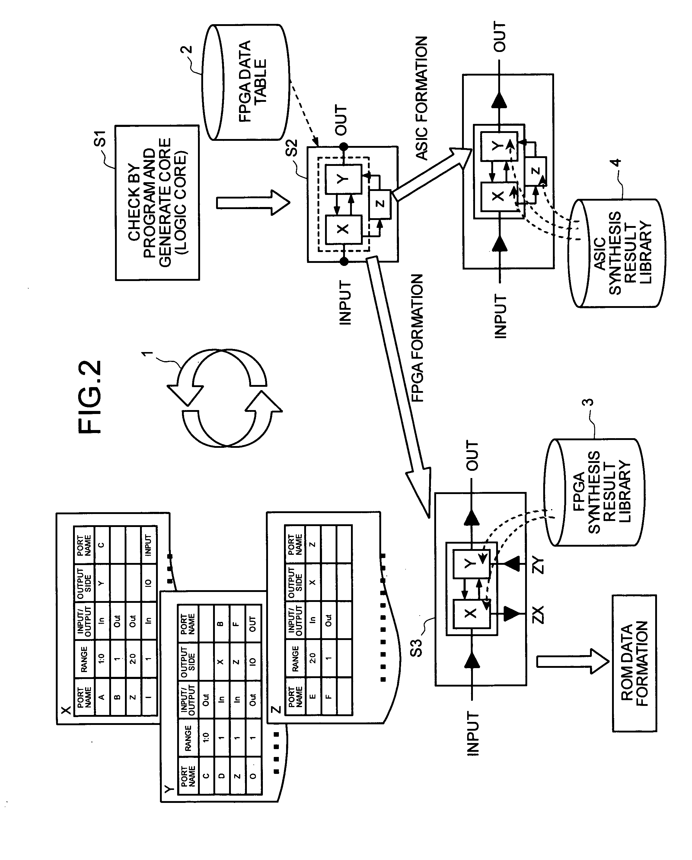
[0090]FIG. 2 is a diagram for explaining the operation of the present invention. An integrated circuit is developed based on shared design data and based on the study of the circuit architecture.

[0091] When designing a function to be realized using the HDL, a chip, being a product itself, is formed of an instance having a certain function. The instance refers to a block with a plurality of functions designed by the HDL, and multiple blocks if a specific block is necessary for realizing a function of the chip.

[0092] In FIG. 2, X, Y, and Z are tables in which a port specification of a block created after studying the circuit architecture is defined according to a defined format. These tables X, Y, and Z are always created when a block is designed, and include block name, instance name, port name, range, input / output, type, instance name on output side, output port name of the instance on the output side, and the like. These data are input manually by a user. It is the key point of th...

second embodiment

[0150] At first, the concept of the concurrent development of the ASIC and the FPGA will be explained with reference to FIG. 12. The characteristic of the concurrent development of the ASIC and the FPGA is that in order to execute prototyping verification by the FPGA concurrently with the implementation designing of the ASIC, ROM data in which an FPGA circuit required for the prototyping verification is recorded, is provided by the implementation design of the ASIC, so that the development of the ASIC and the FPGA can be made seamless.

[0151] In the concurrent development of the ASIC and the FPGA, the prototyping verification by the FPGA is taken into consideration during the study of circuit architecture, division of functions to be realized in a circuit to be realized having a suitable expected size and hierarchization of functions due to structural difference between the ASIC and the FPGA is carried out, to thereby create a common functional block configuration between the ASIC a...


PUM


Abstract

A method for developing integrated circuits includes generating a core (logic core) in an HDL format readable by a logic synthesis tool, from an ASIC core (logic core) made of ports of blocks and port connection information, creating a temporary chip design from chip terminal information to generate a terminal in the temporary chip design, generating a design identical to that created, as a cell within the design created, connecting a design port with a cell port, wherein a name of the design port is identical to a name of the cell port, inserting an I / O buffer, depending on the device technology, into a net between the ports connected, replacing the cell by the core (logic core) created to gerate a netlist, and expanding a hierarchy of the design, being the top hierarchy.

Description

TECHNICAL FIELD [0001] The present invention relates to a programmable logic device forming method for development of integrated circuits, and a development method for developing integrated circuits, a program storage medium for storing the development method for integrated circuits, a controller for a logic synthesis tool, a concurrent development system, a concurrent development program, and a concurrent development method for concurrent development of the ASIC and the programmable logic device, which enable seamless and concurrent development of the ASIC and the programmable logic device, ensure the design quality while reducing the development period, human resources, and development cost. BACKGROUND ART [0002] In the manufacturing procedure of integrated circuits, the specifications are determined, and designing is performed according to the specification, after having examined carefully if anything has been overlooked. FIG. 11 is a flowchart of the procedure for designing inte...

Claims


Application Information

Patent Timeline
Patent Type & Authority Applications(United States)
IPC IPC(8): G06F17/50
CPCG06F17/5045G06F30/30H01L21/82H03K19/173
Inventor KOGA, CHIAKITSUDA, MASAYUKINAKAYAMA, AKITSUGU
Owner FUJITSU LTD
Why Eureka
Try Eureka