Composite optical lithography method for patterning lines of significantly different widths

a technology of optical lithography and patterning lines, which is applied in the direction of photo-taking processes, printing, instruments, etc., can solve the problem that complex lithographic exposure tools may cost more to make and opera

Inactive Publication Date: 2005-04-07
INTEL CORP
View PDF27 Cites 58 Cited by
  • Summary
  • Abstract
  • Description
  • Claims
  • Application Information

AI Technical Summary

Problems solved by technology

Complex lithographic exposure tools may cost more to make and operate.

Method used


Image

  • Composite optical lithography method for patterning lines of significantly different widths
  • Composite optical lithography method for patterning lines of significantly different widths
  • Composite optical lithography method for patterning lines of significantly different widths

Examples


Embodiment Construction

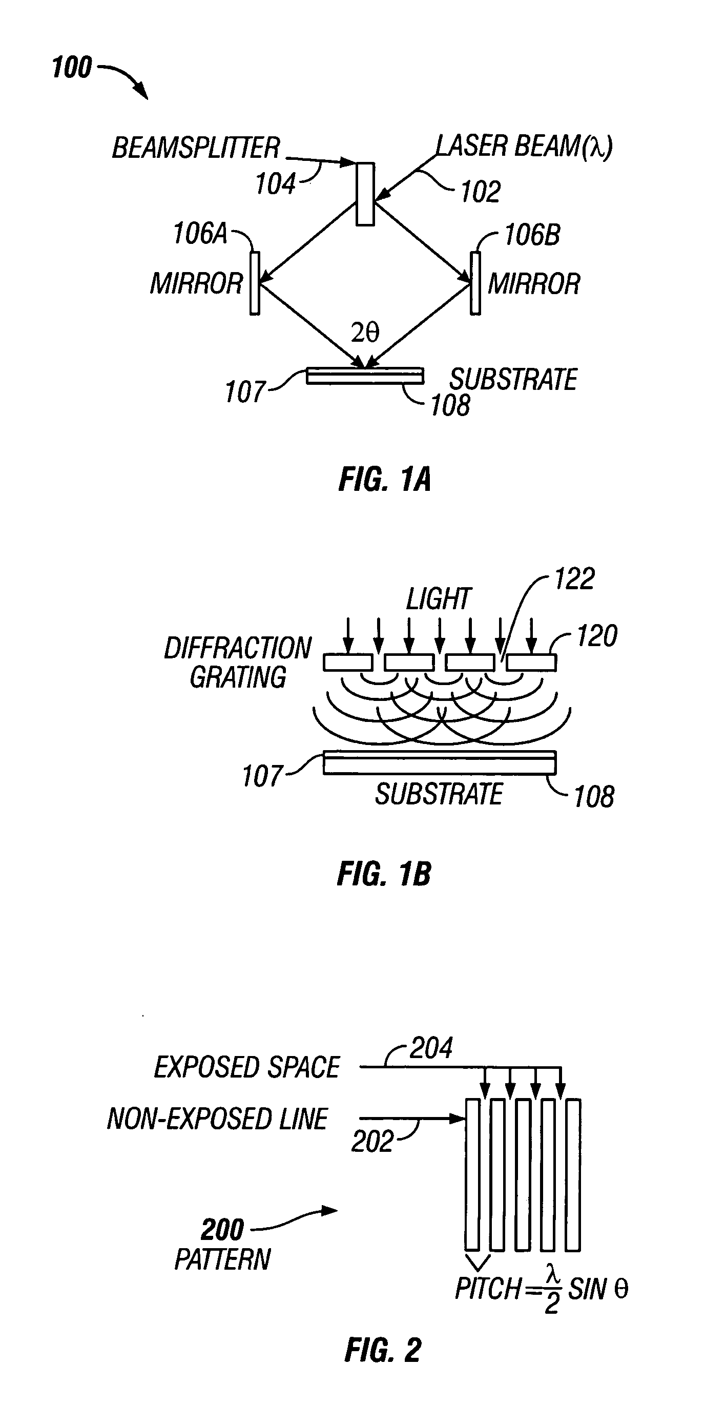
A conventional patterning technique may use expensive, diffraction-limited, high numerical aperture (NA), high aberration-corrected lens or tools equipped with complex illumination. A conventional patterning technique may also use complicated and expensive masks, which employ various phase shifters and complex optical proximity corrections (OPC).

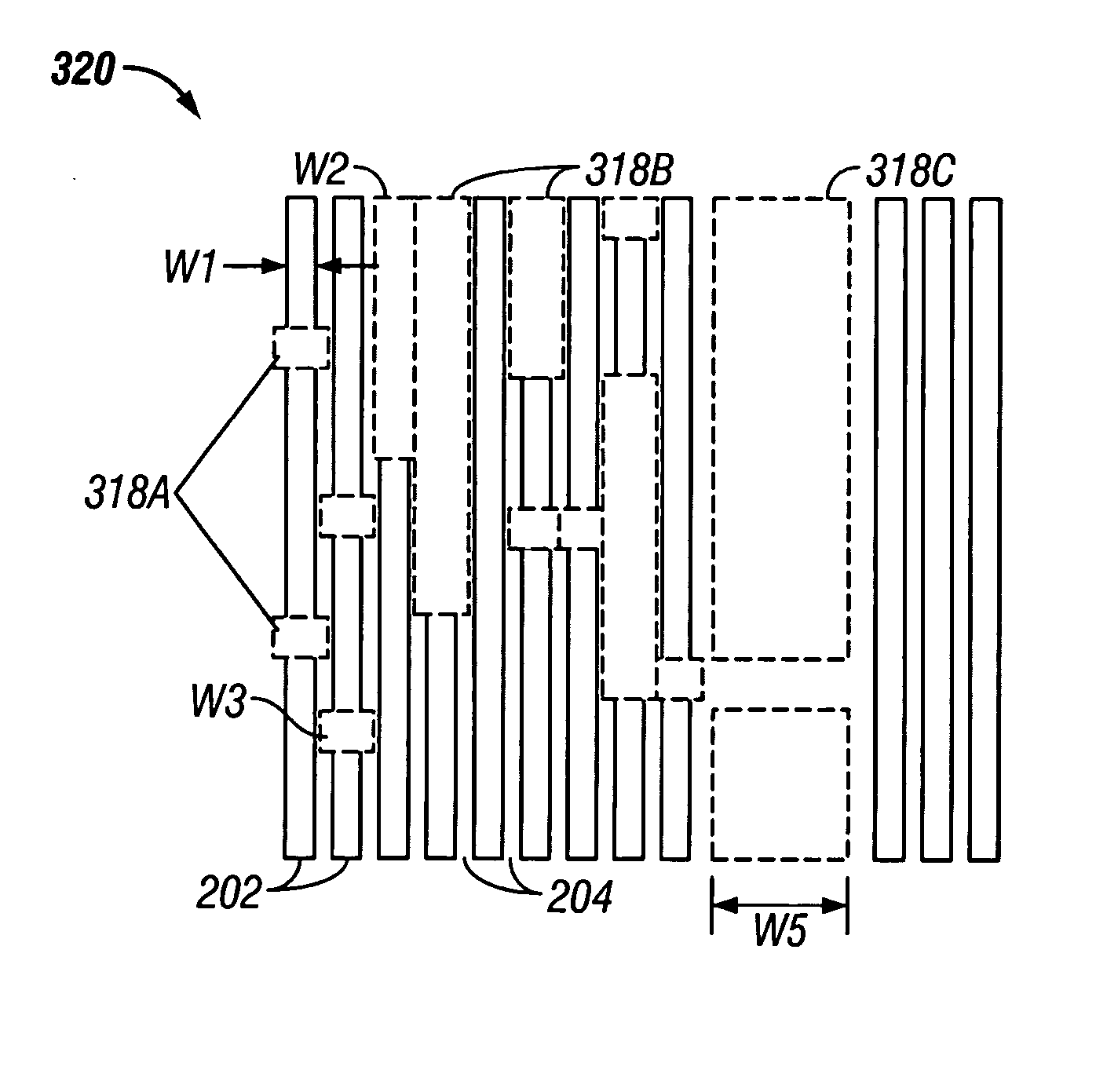
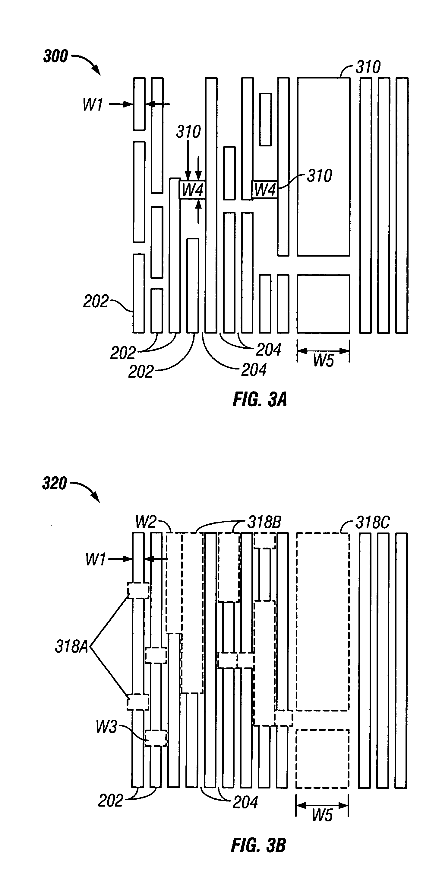
The present application relates to a composite optical lithography patterning technique, which may form smaller integrated circuit features compared to conventional lithography techniques. The composite patterning technique may provide a higher density of integrated circuit features for a given area on a substrate.

The composite patterning technique may include two or more lithography processes. A first lithography process may use interference lithography to form a periodic alternating pattern of lines of substantially equal width and spaces on a first photoresist. A second lithography process may use a non-interference lithography techniq...


PUM

PropertyMeasurementUnit
widthaaaaaaaaaa
areaaaaaaaaaaa
wavelengthaaaaaaaaaa

Abstract

A composite patterning technique may include three lithography processes. A first lithography process forms a periodic pattern of alternating continuous lines of substantially equal width and spaces on a first photoresist. A second lithography process uses a non-interference lithography technique to break continuity of the patterned lines and form portions of desired integrated circuit features. The first photoresist may be developed. A second photoresist is formed over the first photoresist. A third lithography process uses a non-interference lithography technique to expose a pattern on the second photoresist and form remaining desired features of an integrated circuit pattern.

Description

BACKGROUND An integrated circuit (IC) manufacturing process may deposit various material layers on a wafer and form a photosensitive resist (photoresist) on the deposited layers. The process may use lithography to transmit light through or reflect light from a patterned reticle (mask) to the photoresist. Light from the reticle transfers a patterned image onto the photoresist. The process may remove portions of the photoresist which are exposed to light. A process may etch portions of the wafer which are not protected by the remaining photoresist to form integrated circuit features. The semiconductor industry may continually strive to reduce the size of transistor features to increase transistor density and to improve transistor performance. This desire has driven a reduction in the wavelength of light used in photolithographic techniques to define smaller IC features in a photoresist. Complex lithographic exposure tools may cost more to make and operate. BRIEF DESCRIPTION OF DRAWI...

Claims


Application Information

Patent Timeline
Patent Type & Authority Applications(United States)
IPC IPC(8): G03F7/20
CPCG03F7/7045G03F7/70408G03F7/094
Inventor BORODOVSKY, YAN
Owner INTEL CORP
Why Eureka
Try Eureka