Semiconductor fabrication apparatus and pattern formation method using the same

a technology of semiconductor fabrication and pattern formation, applied in the direction of photomechanical equipment, instruments, printers, etc., can solve the problems of disadvantageous increase of the whole cost of semiconductor fabrication and increase of exposure cost, and achieve the effect of low cos

Inactive Publication Date: 2005-04-07
PANASONIC CORP
View PDF1 Cites 213 Cited by
  • Summary
  • Abstract
  • Description
  • Claims
  • Application Information

AI Technical Summary

Benefits of technology

[0009] An object of the invention is solving the problem by performing pattern formation through the immersion lithography at low cost.

Problems solved by technology

As described above, a large amount of liquid is consumed, the cost for the exposure is increased.
In addition, it is necessary to subject the liquid to waste solution processing before it is discarded, and hence, the whole cost for the semiconductor fabrication is disadvantageously increased.

Method used


Image

  • Semiconductor fabrication apparatus and pattern formation method using the same
  • Semiconductor fabrication apparatus and pattern formation method using the same
  • Semiconductor fabrication apparatus and pattern formation method using the same

Examples


embodiment 1

[0043][0043] Embodiment 1

[0044] Embodiment 1 of the invention will now be described with reference to the accompanying drawings. [0045] (Semiconductor Fabrication Apparatus)

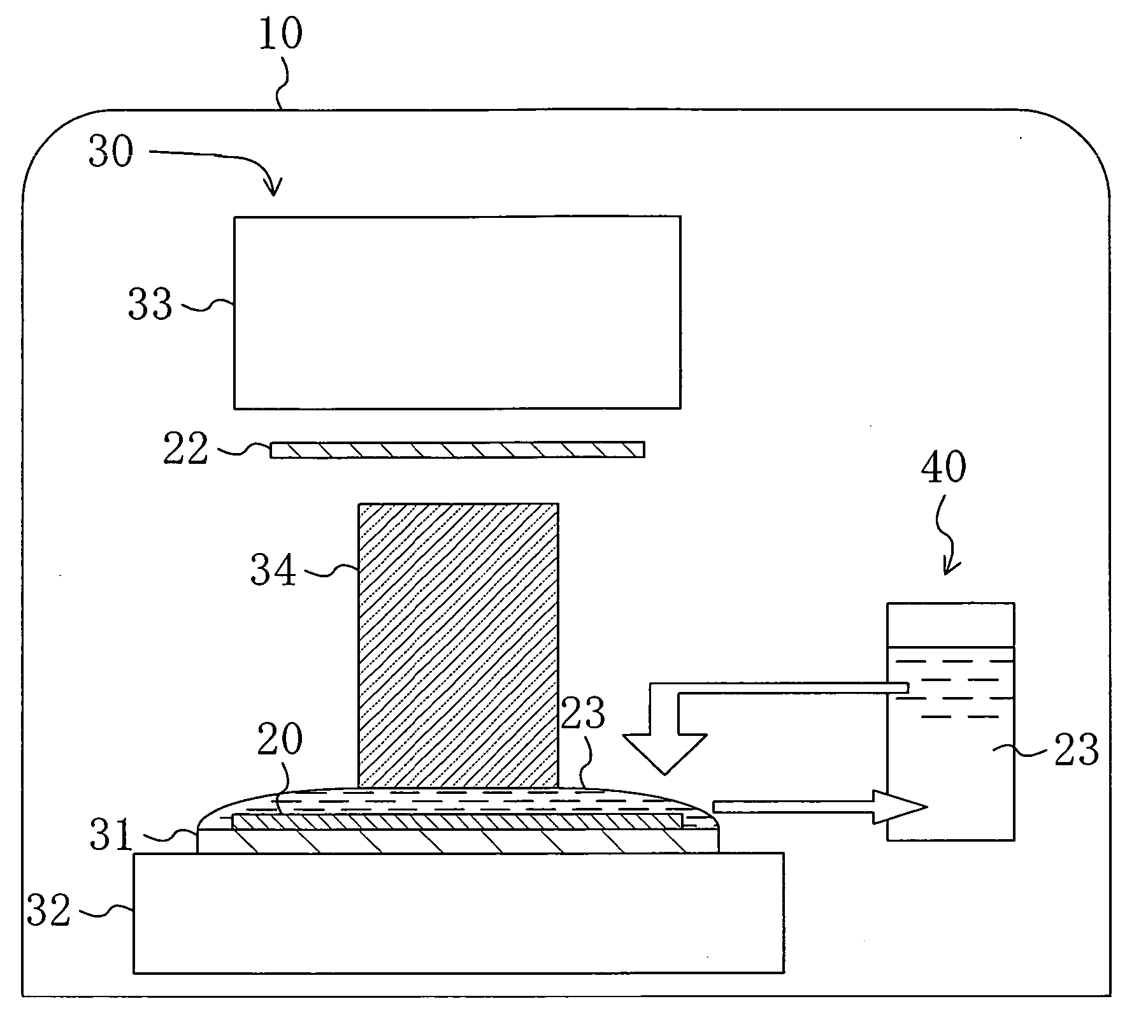
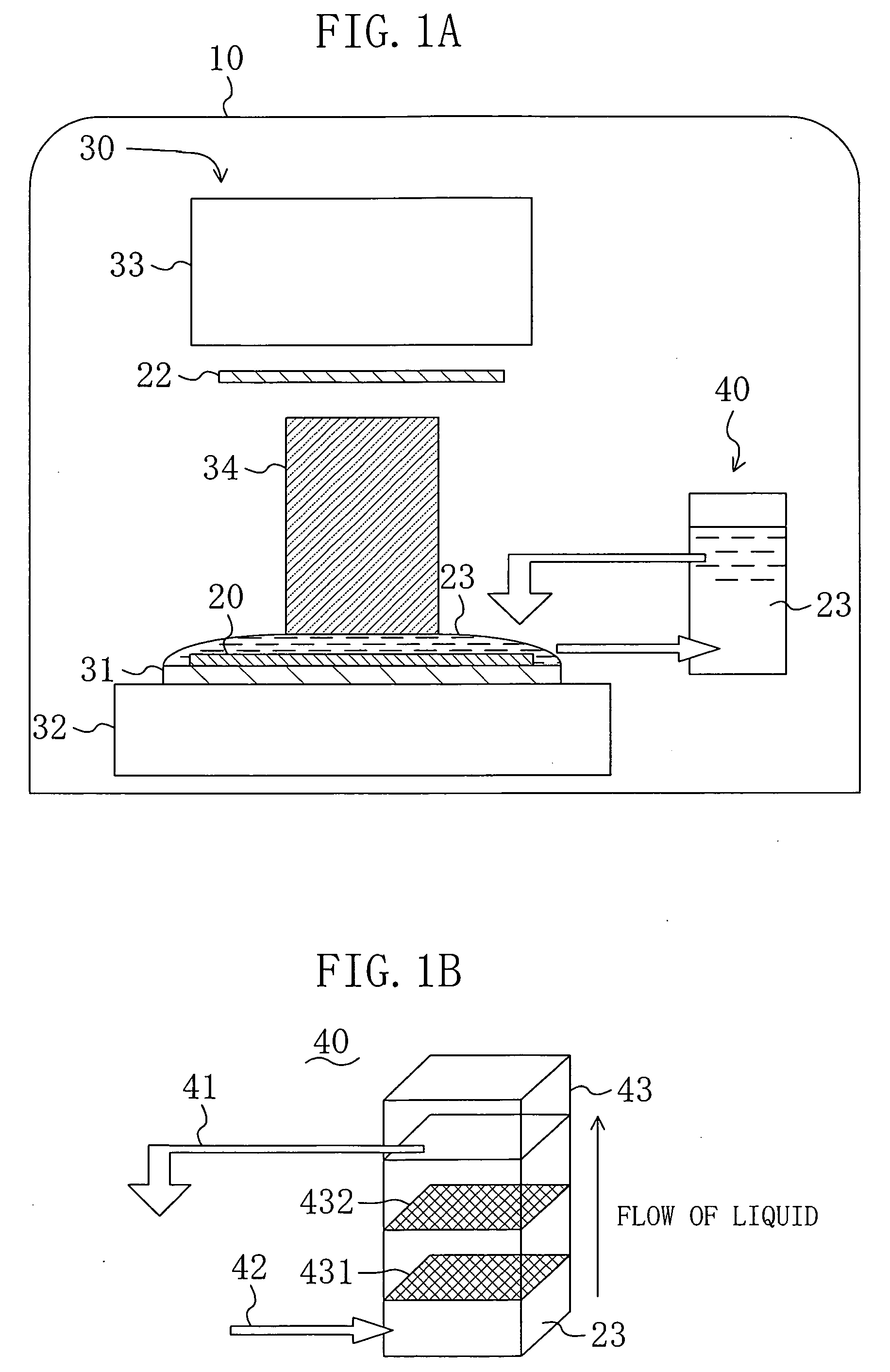
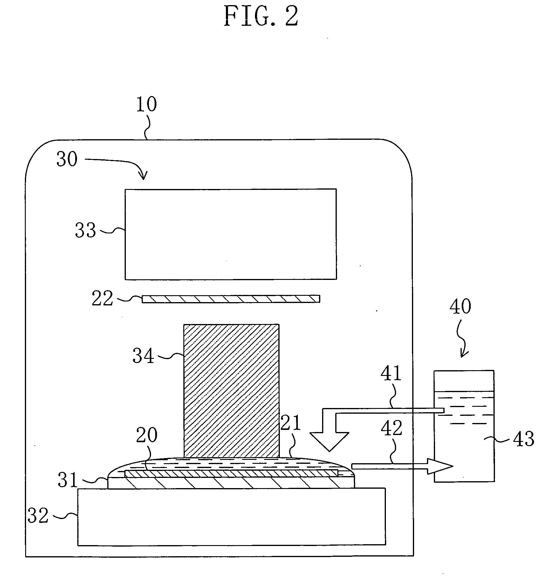
[0046]FIGS. 1A and 1B show a semiconductor fabrication apparatus used for realizing a pattern formation method employing immersion lithography according to Embodiment 1 of the invention, and more specifically, FIG. 1A is a schematic cross-sectional view of a principal portion of the semiconductor fabrication apparatus and FIG. 1B is a schematic perspective view of a liquid recycle section of the semiconductor fabrication apparatus.

[0047] As shown in FIG. 1A, the semiconductor fabrication apparatus of Embodiment 1 includes an exposure section 30 that is provided within a chamber 10 for exposing a design pattern on a resist film (not shown) applied on a wafer 20, and a liquid recycle section 40 that supplies a liquid 23, which is used in the immersion lithography for increasing the numerical aperture of exposing...

embodiment 2

[0070] Furthermore, the liquids 23, 23A and 23B used for the immersion lithography may be water instead of perfluoropolyether. [0071] Embodiment 2

[0072] Embodiment 2 of the invention will now be described.

[0073] Also in the conventional exposure system employing the pooling method shown in FIG. 7B, it is necessary to periodically exchange the liquid 250 for immersion as described above. This is because a resist film deposited on the wafer 200 is always in contact with the liquid 250 during the exposure in portions other than exposed portions, and the contact area between the liquid 250 and the resist film is large and the contact time is long.

[0074] In general, a resist film is made from a mixture of a plurality of materials, and an acid is generated from the resist film during the exposure. Accordingly, even when the liquid 250 for immersion is difficult to dissolve the resist film, it is difficult to completely prevent the acid generated from the resist film and compounds inclu...


PUM

PropertyMeasurementUnit
thicknessaaaaaaaaaa
temperatureaaaaaaaaaa
widthaaaaaaaaaa

Abstract

The semiconductor fabrication apparatus of this invention includes an exposure section provided within a chamber for exposing a design pattern on a resist film applied on a wafer, and a liquid recycle section for supplying, onto the wafer, a liquid for use in immersion lithography for increasing the numerical aperture of exposing light during exposure while recycling the liquid. The liquid recycle section includes a liquid supply part for supplying the liquid onto the resist film of the wafer, a liquid discharge part for discharging and recovering the liquid from above the wafer, and an impurity removal part for containing the liquid and removing an impurity included in the liquid.

Description

BACKGROUND OF THE INVENTION [0001] The present invention relates to a semiconductor fabrication apparatus for use in fabrication process and the like for semiconductor devices and a pattern formation method using the semiconductor fabrication apparatus. [0002] In accordance with the increased degree of integration of semiconductor integrated circuits and downsizing of semiconductor devices, there are increasing demands for further rapid development of lithography technique. Currently, pattern formation is carried out through photolithography using exposing light of a mercury lamp, KrF excimer laser, ArF excimer laser or the like, and use of F2 laser lasing at a shorter wavelength is being examined. However, since there remain a large number of problems in exposure systems and resist materials, photolithography using exposing light of a shorter wavelength has not been put to practical use. [0003] In these circumstances, immersion lithography has been recently proposed for realizing f...

Claims


Application Information

Patent Timeline
Patent Type & Authority Applications(United States)
IPC IPC(8): G03F7/20H01L21/027
CPCG03F7/70341
Inventor ENDO, MASAYUKISASAGO, MASARU
Owner PANASONIC CORP
Why Eureka
Try Eureka