Exponential channelized timer

Inactive Publication Date: 2005-04-14
AVAGO TECH WIRELESS IP SINGAPORE PTE
View PDF4 Cites 35 Cited by
  • Summary
  • Abstract
  • Description
  • Claims
  • Application Information

AI Technical Summary

Benefits of technology

[0009] In accordance with the present invention, an integrated circuit system and method are provided for efficiently generating multiple, independent timer request signals where each timer request signal may have its own time-out setting. To generate multiple time-out signals for a plurality of channels, a free-running multi-bit timer runs in a loop. For a given channel, a selected bit position of the free-running timer is monitored under control of a programmable timer control register, and a pulse is generated whenever a transition is observed in the selected bit position of the free-running timer. The pulse serves as the time-out signal for the given channel. To assist with timer request generation, a multiplexer and timer control register are associated with each of channel for

Problems solved by technology

As the number of channels increases, the unwield

Method used


Image

  • Exponential channelized timer
  • Exponential channelized timer
  • Exponential channelized timer

Examples


Embodiment Construction

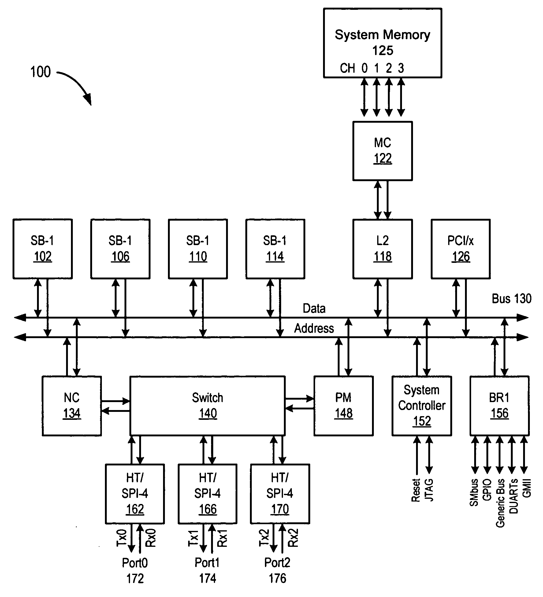
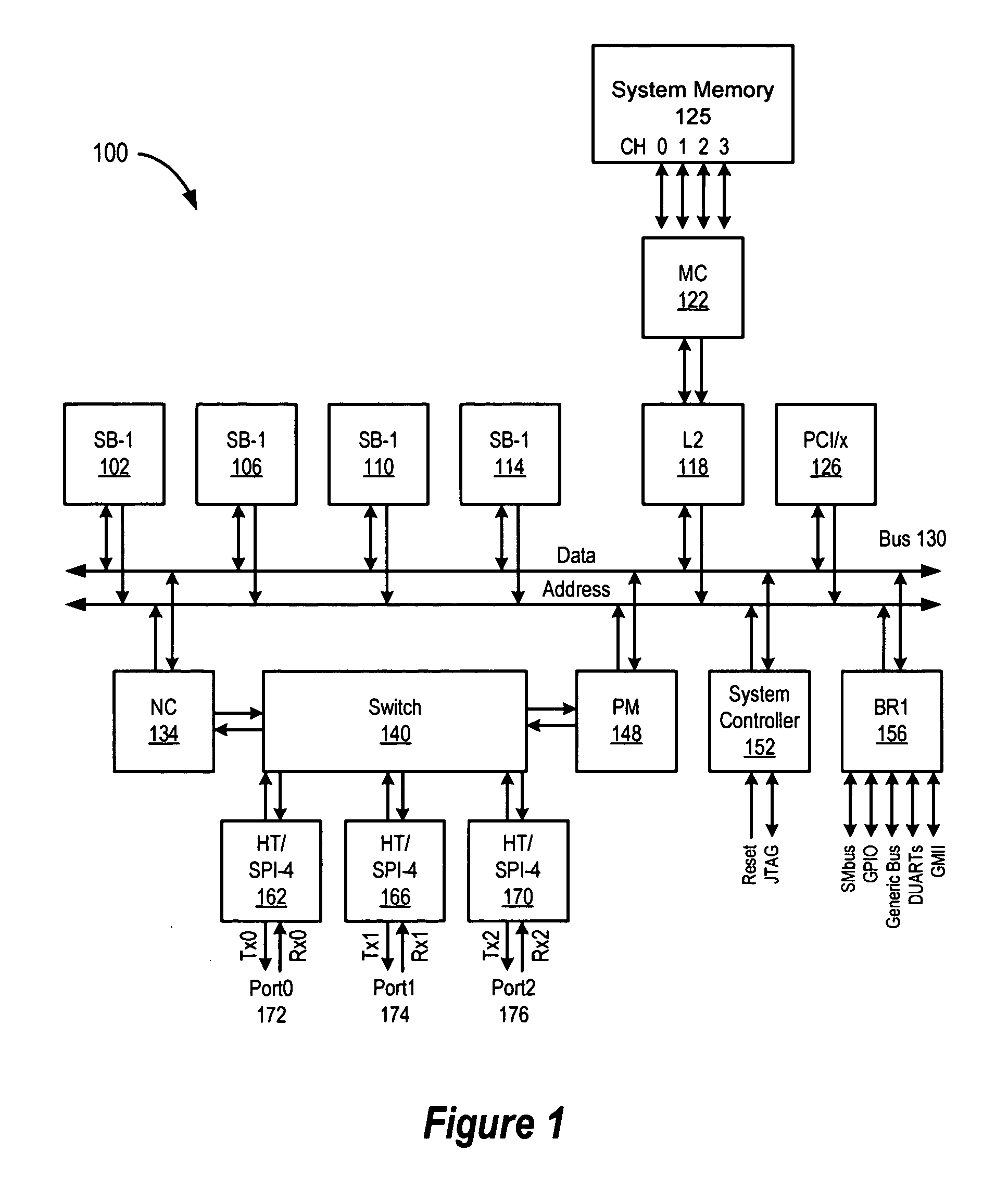
[0027] An apparatus and method in accordance with the present invention provide a system for routing incoming packets through a multiprocessor switching system-on-a-chip. A system level description of the operation of an embodiment of the multiprocessor switching system of the present invention is shown in FIG. 1 which depicts a schematic block diagram of a multiprocessor device 100 in accordance with the present invention. The multiprocessor device 100 may be an integrated circuit or it may be constructed from discrete components. The multiprocessor device 100 includes a plurality of processing units 102, 106, 110, 114, cache memory 118, memory controller 122, which interfaces with on and / or off-chip system memory 125, an internal bus 130, a node controller 134, a switching module 140, a packet manager 148, a system controller 152 and a plurality of configurable packet based interfaces 162, 166, 170, such as three flexible HyperTransport / SPI-4 Phase 2 links.

[0028] As shown in FIG....


PUM


Abstract

A multiprocessor switching device substantially implemented on a single CMOS integrated circuit is described in connection with a channelized timer for use in controlling the issuance of signals to the processor(s) or control logic (such as interrupts, descriptors, etc.) that that identify system-related functions for a plurality of channels. Using control registers to select an individual bit of a multi-bit counter, a timing interval pulse is provided for prompting signal generation that is otherwise subject to a minimum count requirement.

Description

RELATED APPLICATIONS [0001] This application is related to U.S. Provisional Patent Application Ser. No. 60 / 380,740, filed May 15, 2002; U.S. Provisional Patent Application Ser. No. 60 / 331,789, filed Nov. 20, 2001; U.S. Provisional Patent Application Ser. No. 60 / 344,713, filed Dec. 24, 2001; U.S. Provisional Patent Application Ser. No. 60 / 348,777, filed Jan. 14, 2002, U.S. Provisional Patent Application Ser. No. 60 / 348,717, filed Jan. 14, 2002, U.S. patent application Ser. No. 10 / 270,016, filed Oct. 11, 2002 and U.S. patent application Ser. No. 10 / 269,666, filed Oct. 11, 2002, each of which is incorporated herein by reference in its entirety.BACKGROUND OF THE INVENTION [0002] 1. Field of the Invention [0003] The present invention is directed in general to data communications. In one aspect, the present invention relates to a method and system for generating timer request signals for multiple channels in a multiprocessor computer device. [0004] 2. Related Art [0005] As is known, commu...

Claims


Application Information

Patent Timeline
IPC IPC(8): H04L29/06
CPCH04L69/28
Inventor ONER, KORAY
Owner AVAGO TECH WIRELESS IP SINGAPORE PTE
Why Eureka
Try Eureka