Double heterojunction light emitting diodes and laser diodes having quantum dot silicon light emitters

a light emitter and laser diode technology, applied in the direction of lasers, semiconductor laser structural details, semiconductor lasers, etc., can solve the problem of relatively inefficient light emitters of silicon

Inactive Publication Date: 2005-04-21
ASTRALUX
View PDF11 Cites 24 Cited by
  • Summary
  • Abstract
  • Description
  • Claims
  • Application Information

AI Technical Summary

Problems solved by technology

However, silicon has an indirect bandgap of about 1.1 eV, which makes silicon a relatively inefficient light emitter.

Method used


Image

  • Double heterojunction light emitting diodes and laser diodes having quantum dot silicon light emitters
  • Double heterojunction light emitting diodes and laser diodes having quantum dot silicon light emitters
  • Double heterojunction light emitting diodes and laser diodes having quantum dot silicon light emitters

Examples


Embodiment Construction

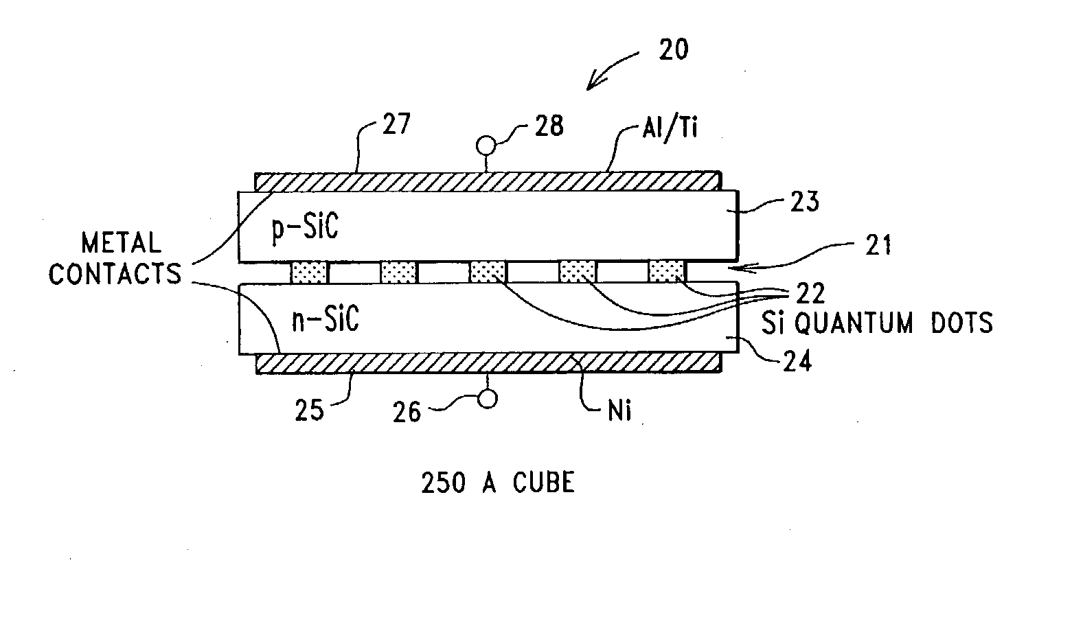
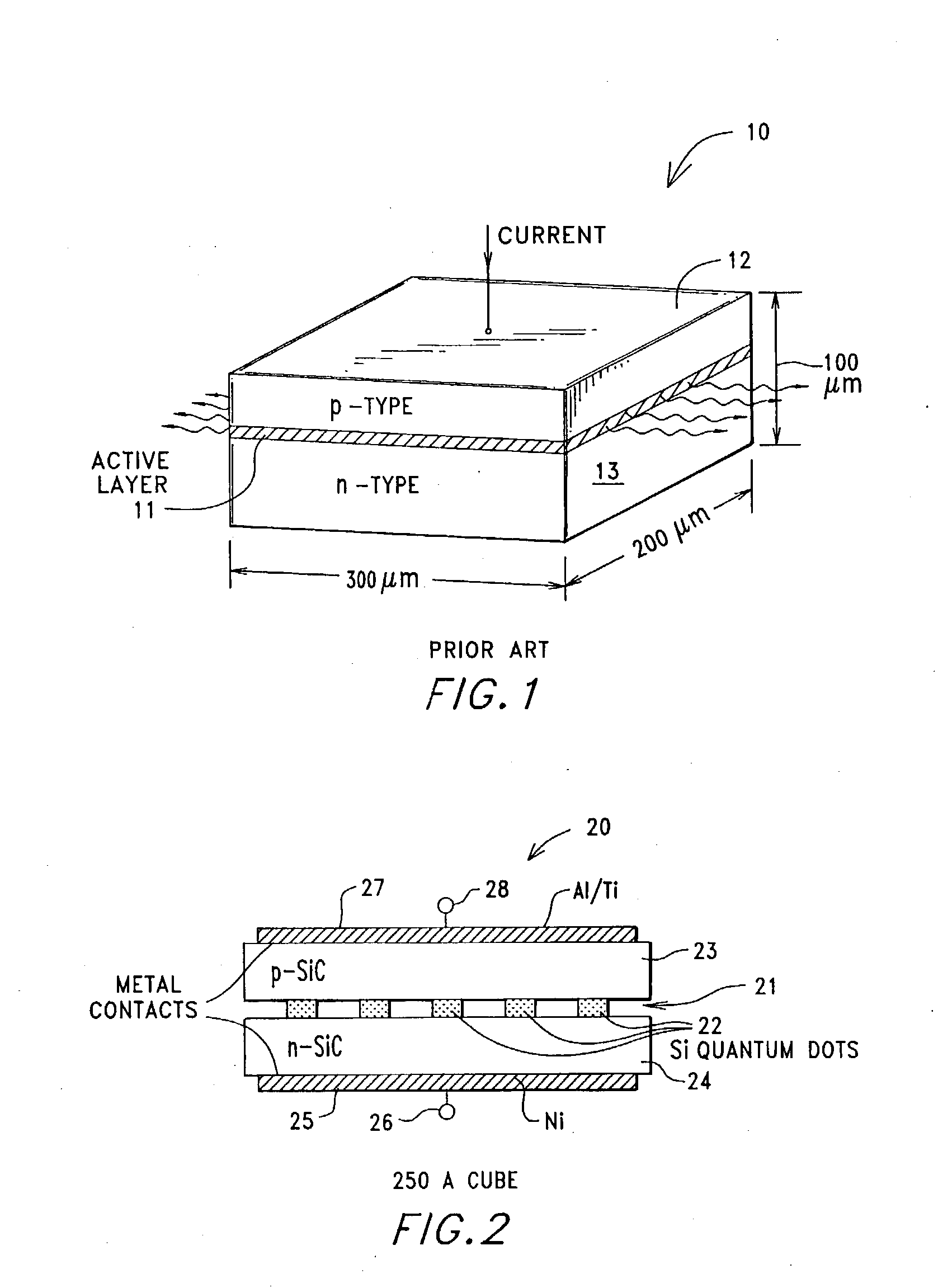
[0025] With reference to FIG. 2, a Si-based DH LED or a Si-based DH LD 20 in accordance with this invention includes a thin (no greater than about 250 Angstroms thick) layer 21 having a plurality of narrow band gap Si QDs 22, wherein Si QD layer 21 is sandwiched between a p-type, wide band gap SiC cladding layer 23 and an n-type wide band gap SiC cladding layer 24.

[0026] DH device 20 also includes a first metal electrical contact 25 and its electrical connection 26, and a second metal electrical contact 27 and its electrical contact 28. Metal contacts 25 and 27 are preferably alloyed at high temperature, for example over 1000 degrees centigrade, thus assuring good ohmic contact to the DH device 20. Nickel (Ni) can be used to form contact 25, whereas aluminum (Al), titanium (Ti) or a Al / Ti alloy can be used to form contact 27.

[0027] The two doped SiC cladding layers 23 and 24 have a wide or large band gap and a small index of refraction, and the two cladding layers 23 and 24 form a...


PUM


Abstract

A direct-wafer-bonded, double heterojunction, light emitting semiconductor device includes an ordered array of quantum dots made of one or more indirect band gap materials selected from a group consisting of Si, Ge, SiGe, SiGeC, 3C—SiC, and hexagonal SiC, wherein the quantum dots are sandwiched between an n-type semiconductor cladding layer selected from a group consisting of SiC, 3C—SiC, 4H—SiC, 6H—SiC and diamond, and a p-type semiconductor cladding layer selected from a group consisting of SiC, 3C—SiC, 4H—SiC, 6H—SiC and diamond. A Ni contact is provided for the n-type cladding layer. An Al, a Ti or an Al / Ti alloy contact is provided for the p-type cladding layer. The quantum dots have a thickness that is no greater than about 250 Angstroms, a width that is no greater than about 200 Angstroms, and a center-to-center spacing that is in the range of from about 10 Angstroms to about 1000 Angstroms.

Description

CROSS REFERENCE TO RELATED APPLICATIONS [0001] This patent application is a division of non-provisional patent application Ser. No. 10 / 273,041, entitled “DOUBLE HETEROJUNCTION LIGHT EMITTING DIODES AND LASER DIODES HAVING QUANTUM DOT SILICON LIGHT EMITTERS”, filed Oct. 17, 2002, and incorporated herein by reference.FIELD OF THE INVENTION [0002] This invention relates to the fabrication of semiconductor devices, and more specifically to the fabrication of silicon-based (Si-based) light emitting diodes (LEDs) and laser diodes (LDs) using nano-patterning and direct wafer bonding techniques. BACKGROUND OF THE INVENTION [0003] As the term is used herein, direct-wafer-bonding is intended to mean a process whereby two smooth and flat surfaces are brought together, in physical contact, in the absence of an intermediate layer or film, and usually with the application of a uniaxial pressure, such that the two flat surfaces are locally attracted to each other by Van der Walls forces, so that t...

Claims


Application Information

Patent Timeline
Patent Type & Authority Applications(United States)
IPC IPC(8): H01L33/00H01L33/06H01L33/34H01S5/02H01S5/30H01S5/34
CPCB82Y20/00H01L33/06H01L33/34H01S5/021Y10S977/95H01S5/3027H01S5/3031H01S5/3036H01S5/3412H01S5/0215
Inventor TORVIK, JOHN TARJE
Owner ASTRALUX
Why Eureka
Try Eureka