Eureka AIR delivers breakthrough ideas for toughest innovation challenges, trusted by R&D personnel around the world.

Platinum stuffed with silicon oxide as a diffusion oxygen barrier for semiconductor devices

a technology of diffusion oxygen and silicon oxide, which is applied in the direction of semiconductor devices, capacitors, electrical devices, etc., can solve the problems of degrading the storage capacity of cell capacitors, degrading the barrier properties, and reducing the series capacitance, and achieves the effect of high dielectric mim storage cell capacitors

Inactive Publication Date: 2005-04-21
MICRON TECH INC
View PDF7 Cites 44 Cited by
  • Summary
  • Abstract
  • Description
  • Claims
  • Application Information

AI Technical Summary

Benefits of technology

[0009] The present invention provides techniques for fabricating an effective oxygen barrier layer in dense semiconductor memory arrays.
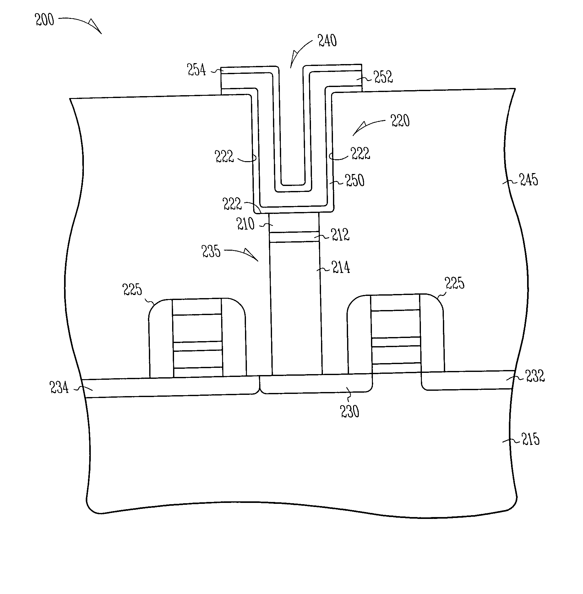
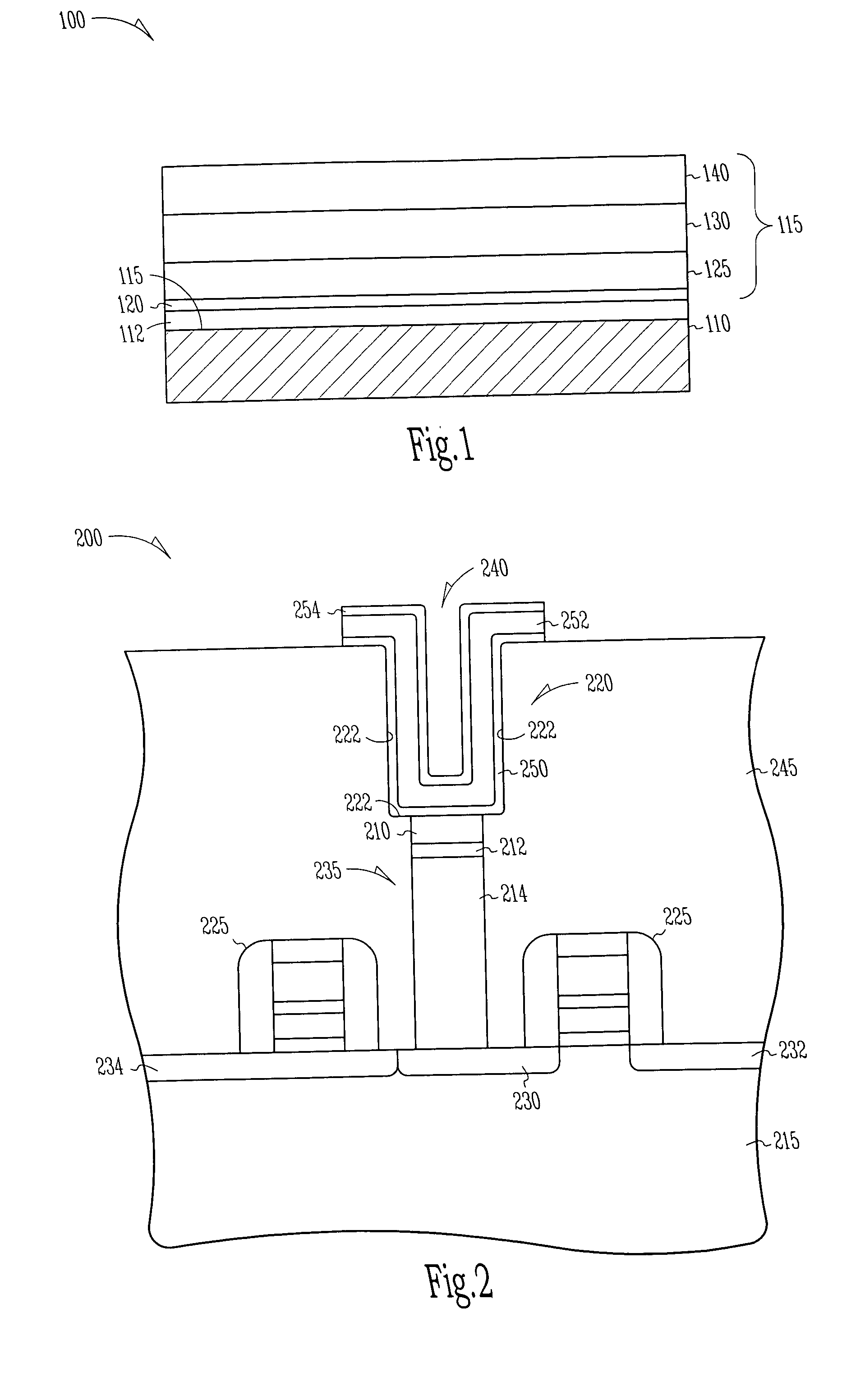
[0010] In one aspect, the invention provides methods for forming a high dielectric MIM storage cell capacitor on a silicon substrate. In one embodiment of the methods, the high dielectric MIM storage cell capacitor is fabricated by forming a barrier layer, including platinum stuffed with silicon oxide over the silicon substrate. A bottom electrode layer is then formed by using platinum over the formed barrier layer. Further, a tantalum oxide insulator layer is formed over the formed platinum layer. A top electrode layer is then formed over the formed tantalum oxide layer.
[0011] In another aspect, the invention provides methods for forming a semiconductor structure including at least one transistor device, on a silicon substrate. In one embodiment of the methods a polysilicon contact is then formed to electrically connect the formed bottom electrode layer in the container with the at least one transistor device. A titanium nitride barrier layer is then formed over the polysilicon contact. An oxygen barrier layer, including platinum stuffed with silicon oxide is then formed over the titanium nitride layer and below the bottom electrode layer. A bottom electrode layer is then formed by using platinum over interior surfaces of a container formed relative to the at least one transistor device in the silicon substrate. Further, a high dielectric insulator layer is formed over the bottom electrode layer. In addition, a top electrode layer is over the formed high dielectric in

Problems solved by technology

This is required since any oxidation of the underlying silicon upon which the capacitor is formed will result in decreased series capacitance thus degrading the storage capacity of the cell capacitor.
This can result in degrading the barrier properties.

Method used


Image

  • Platinum stuffed with silicon oxide as a diffusion oxygen barrier for semiconductor devices
  • Platinum stuffed with silicon oxide as a diffusion oxygen barrier for semiconductor devices
  • Platinum stuffed with silicon oxide as a diffusion oxygen barrier for semiconductor devices

Examples


Embodiment Construction

[0023] In the following detailed description, reference is made to various specific embodiments in which the invention may be practiced. These embodiments are described with sufficient detail to enable those skilled in the art to practice the invention, and it is to be understood that other embodiments may be employed, and that structural, logical, electrical, and process changes may be made without departing from the teachings of the invention.

[0024] In the foregoing description of the preferred embodiments, various features of the invention are grouped together in a single embodiment for the purpose of streamlining the disclosure. This method of disclosure is not to be interpreted as reflecting an intention that the claimed invention requires more features than are expressly recited in each claim. Rather, as the following claims reflect, inventive aspects lie in less than all features of a single disclosed embodiment. Thus, the following claims are hereby incorporated into the de...


PUM


Abstract

The present invention provides techniques to fabricate high dielectric MIM storage cell capacitors. In one embodiment, this is accomplished by forming a silicon contact is then formed to electrically connect the formed bottom electrode layer in the container with the at least one associated transistor device. A titanium nitride barrier layer is then formed over the silicon contact. An oxygen barrier layer including platinum stuffed with silicon oxide is then formed over the titanium nitride layer and below the bottom electrode layer. A bottom electrode layer is then formed using platinum over interior surfaces of a container formed relative to at lest one associated transistor device on a silicon substrate. Further, a high dielectric insulator layer is formed over the bottom electrode layer. A top electrode layer is then formed over the high dielectric insulator layer.

Description

[0001] This application is a Divisional of U.S. application Ser. No. 10 / 230,605, filed Aug. 29, 2002 which is incorporated herein by reference.FIELD OF THE INVENTION [0002] The present invention relates to semiconductor devices and, in particular, to diffusion barrier layers in dense semiconductor memory arrays. BACKGROUND OF THE INVENTION [0003] In the fabrication of integrated circuits, various conductive layers are used. For example, during the formation of semiconductor devices, such as dynamic random access memories (DRAMs), static random access memories (SRAMs), ferroelectric (FE) memories, etc., conductive materials are used in the formation of storage cell capacitors and also may be used in interconnection structures, for example, conductive layers in contact holes, vias, etc. In many applications, it is preferable that the material used provides effective diffusion barrier characteristics. [0004] For example, effective diffusion barrier characteristics are required for cond...

Claims


Application Information

Patent Timeline
IPC IPC(8): H01L21/02H01L21/285H01L21/768H01L21/8246
CPCH01L21/28562H01L21/7687H01L27/10855H01L29/78H01L27/11507H01L28/65H01L28/75H01L27/11502H10B12/0335H10B53/30H10B53/00
Inventor MARSH, EUGENE P.
Owner MICRON TECH INC
Why Eureka
Eureka Blog
Learn More