Programmable logic device for wireless local area network

a logic device and wireless local area network technology, applied in the field of programmable logic devices, can solve the problems of affecting the use of fpgas on high-speed communication applications, affecting the interfacing with other interfaces, and reducing the gate count, so as to facilitate user access to such an interface, facilitate communication, and facilitate interfacing to other interfaces.

Active Publication Date: 2005-04-21
XILINX INC
View PDF13 Cites 67 Cited by
  • Summary
  • Abstract
  • Description
  • Claims
  • Application Information

AI Technical Summary

Benefits of technology

[0010] Programmability facilitates interfacing to other interfaces, while a having a common interface hardwired or embedded facilitates communication between systems. Examples of hardwired interfaces include USB 1.1, USB 2.0, IEEE 1394, Ethernet, IEEE 802.11a and HiperLAN2, among others. A hardwired interface may exist outside of and / or internal to an FPGA, where such an FPGA may be programmed as a medium access control layer. Moreover, such an FPGA may be programmed as an interface layer between such a medium access control layer and a physical layer. For example, between Ethernet physical and medium access control layers conventionally there is a MII (Media Independent Interface). This facilitates user access to such an interface through programming an FPGA.

Problems solved by technology

Even though FPGAs are very flexible and can be used to implement many circuits, they have some performance limitations, such as longer signal delays and lower gate counts.
These limitations hinder use of FPGAs on high-speed communication applications, namely, those communication applications with real-time processing of information.
Unfortunately, communication circuits implemented as ASICs have several disadvantages.
One such disadvantage is the time-to-market risks associated with the relatively long cycle time necessary for the implementation of a new ASIC design.
An additional disadvantage of using ASICs for communication circuits is that ASICs are “hardwired” and thus conventionally are not reconfigurable for a new application or application upgrade.
However, the data link layer of each of these technologies is different.
However, unknown future unification to a single standard, namely, either IEEE 802.11a or HiperLAN2, is causing concern among those deciding on which version of OFDM to implement in their products.
In addition, nonconformance to a single standard is hampering benefits associated with economies of scale.

Method used


Image

  • Programmable logic device for wireless local area network
  • Programmable logic device for wireless local area network
  • Programmable logic device for wireless local area network

Examples


Embodiment Construction

[0027] The present invention relates generally to programmable logic devices, and more particularly to programmable logic devices configured for wireless communication. In the following description, numerous specific details are set forth in order to provide a more thorough understanding of the present invention. However, it will be apparent to one skilled in the art that the present invention may be practiced without one or more of these specific details. In other instances, well-known features have not been described in detail in order to avoid obscuring the present invention.

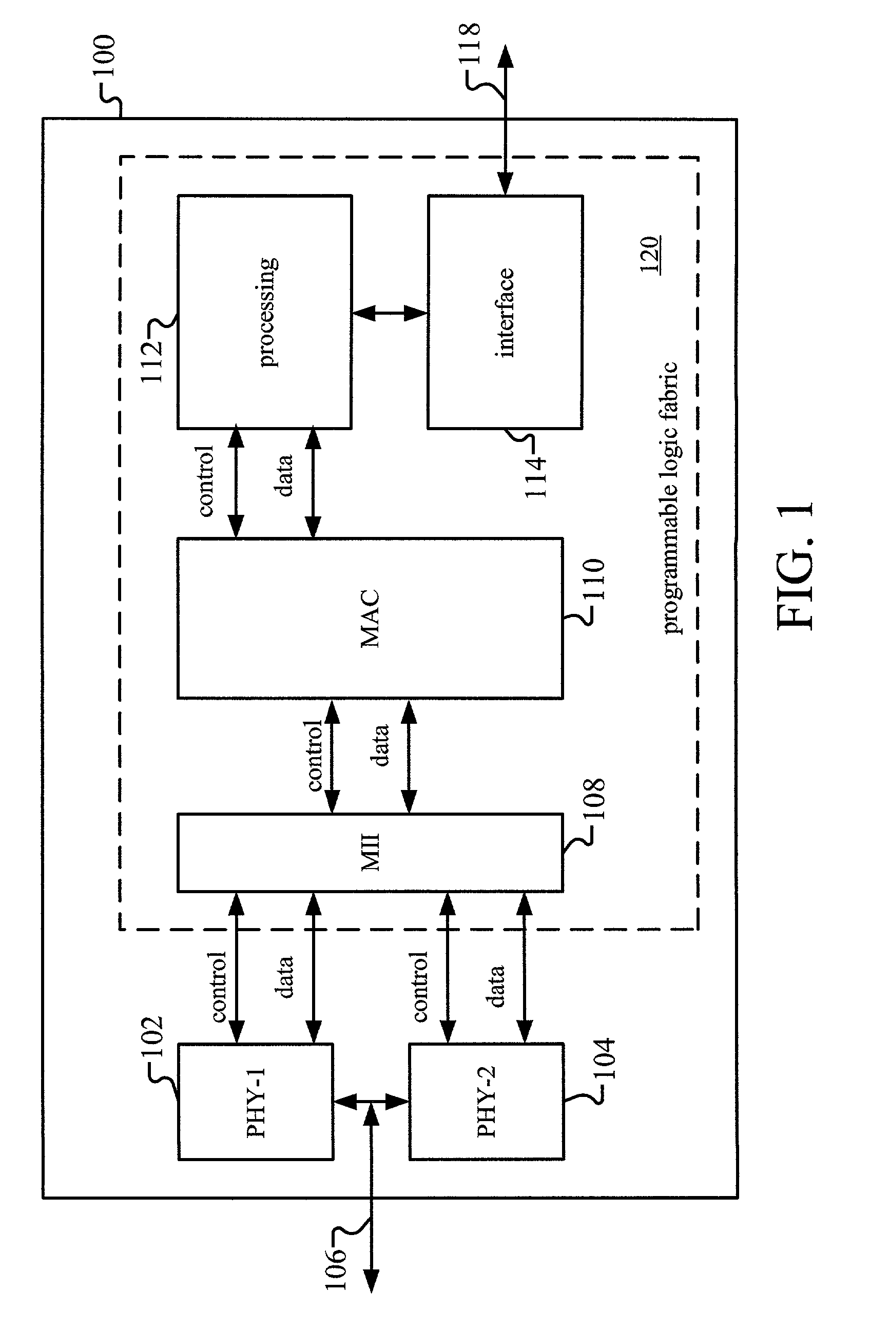
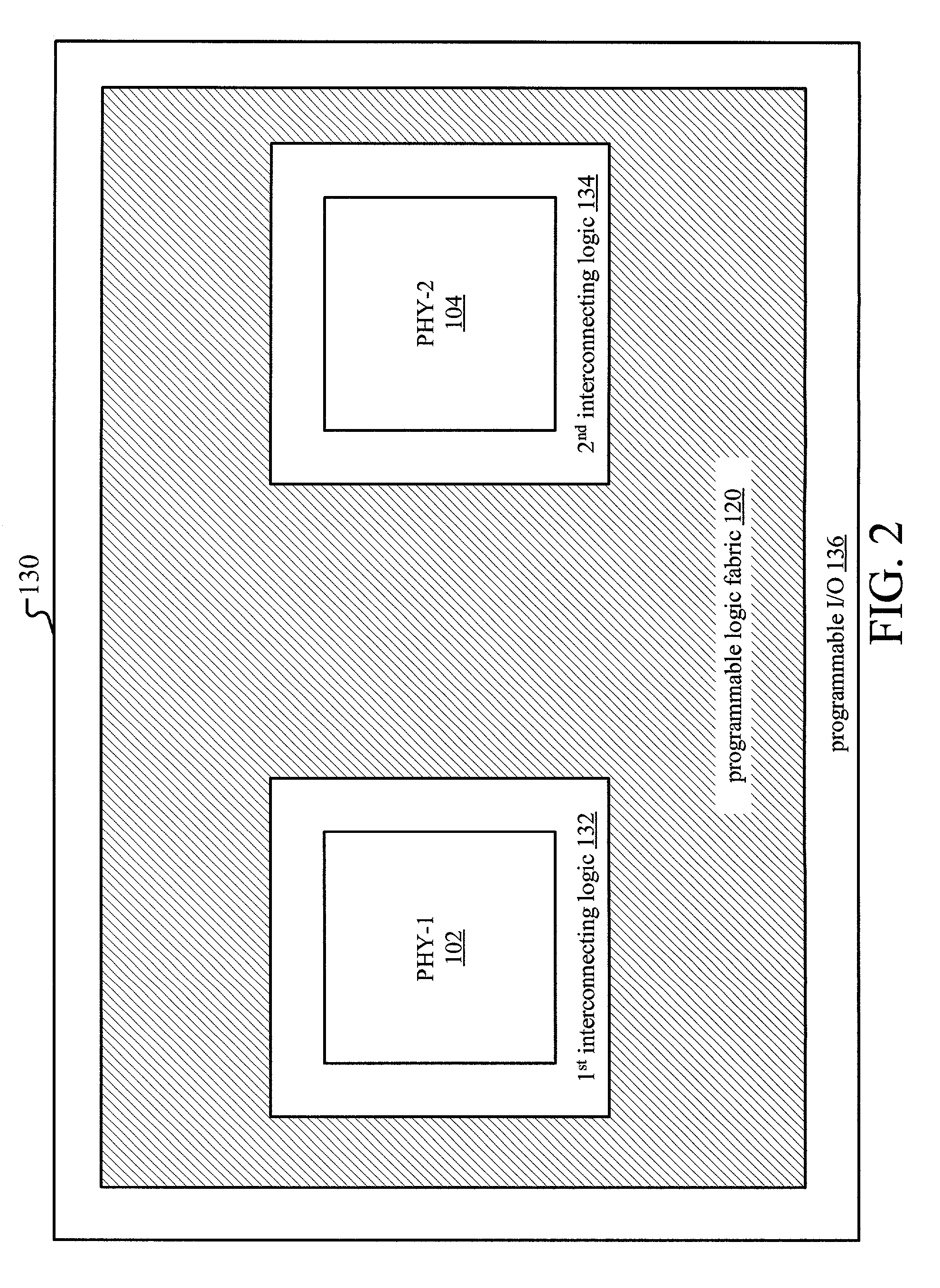
[0028]FIG. 1 is a block diagram of a communication integrated circuit 100 of the present invention. Integrated circuit 100 contains two physical layer (PHY) components (102 and 104) that are connected to a signal line 106. Signal line 106 provides a communication link between integrated circuit 100 and external data of a physical medium. Each PHY communicates with a media independent interface (MII) componen...


PUM


Abstract

Method and apparatus for a wireless local area network programmable logic device is described. More particularly, a field programmable gate array (FPGA) is coupled to memory having programming instructions for configuring the FPGA with a medium access layer selected from more than one type of medium access layers. A physical layer is hardwired or embedded on the FPGA, or a separate integrated circuit for the physical layer is used. Additionally, the memory comprises programming instructions for a baseband controller, and may include programming instructions for a baseband processor, for configuring the FPGA in accordance therewith. In this manner, a single physical layer may be used with an FPGA to provide a multi-platform application specific standard product (ASSP). This is especially advantageous for providing multi-platform devices for use in countries or applications where one or more standards may be employed.

Description

BACKGROUND OF THE INVENTION [0001] 1. Field of the Invention [0002] The present invention relates generally to programmable logic devices, and more particularly to programmable logic devices configured for wireless communication. [0003] 2. Description of the Related Art [0004] Programmable logic devices exist as a well-known type of integrated circuit (IC) that may be programmed by a user to perform specified logic functions. There are different types of programmable logic devices, such as programmable logic arrays (PLAs) and complex programmable logic devices (CPLDs). One type of programmable logic devices, called a field programmable gate array (FPGA), is very popular because of a superior combination of capacity, flexibility and cost. An FPGA typically includes an array of configurable logic blocks (CLBs) surrounded by a ring of programmable input / output blocks (IOBs). The CLBs and IOBs are interconnected by a programmable interconnect structure. The CLBs, IOBs, and interconnect ...

Claims


Application Information

Patent Timeline
Patent Type & Authority Applications(United States)
IPC IPC(8): H04L12/28H04L29/06
CPCH04L12/5692H04L69/18H04L29/06H04L9/40
Inventor DHIR, AMITRANGASAYEE, KRISHNA
Owner XILINX INC
Why Eureka
Try Eureka