
Channel-based testing of communication link

a communication link and channel-based technology, applied in the field of high-speed communication links, can solve the problems of inability to guarantee an acceptable ber in any particular implementation, inability to accurately predict the exact application and environment in which such components will be used, and inability to perform at-speed test and diagnosis. to achieve the effect of facilitating problem determination and corrective action recommendation

Inactive Publication Date: 2005-04-21
IBM CORP
View PDF10 Cites 19 Cited by
  • Summary
  • Abstract
  • Description
  • Claims
  • Application Information

AI Technical Summary

Benefits of technology

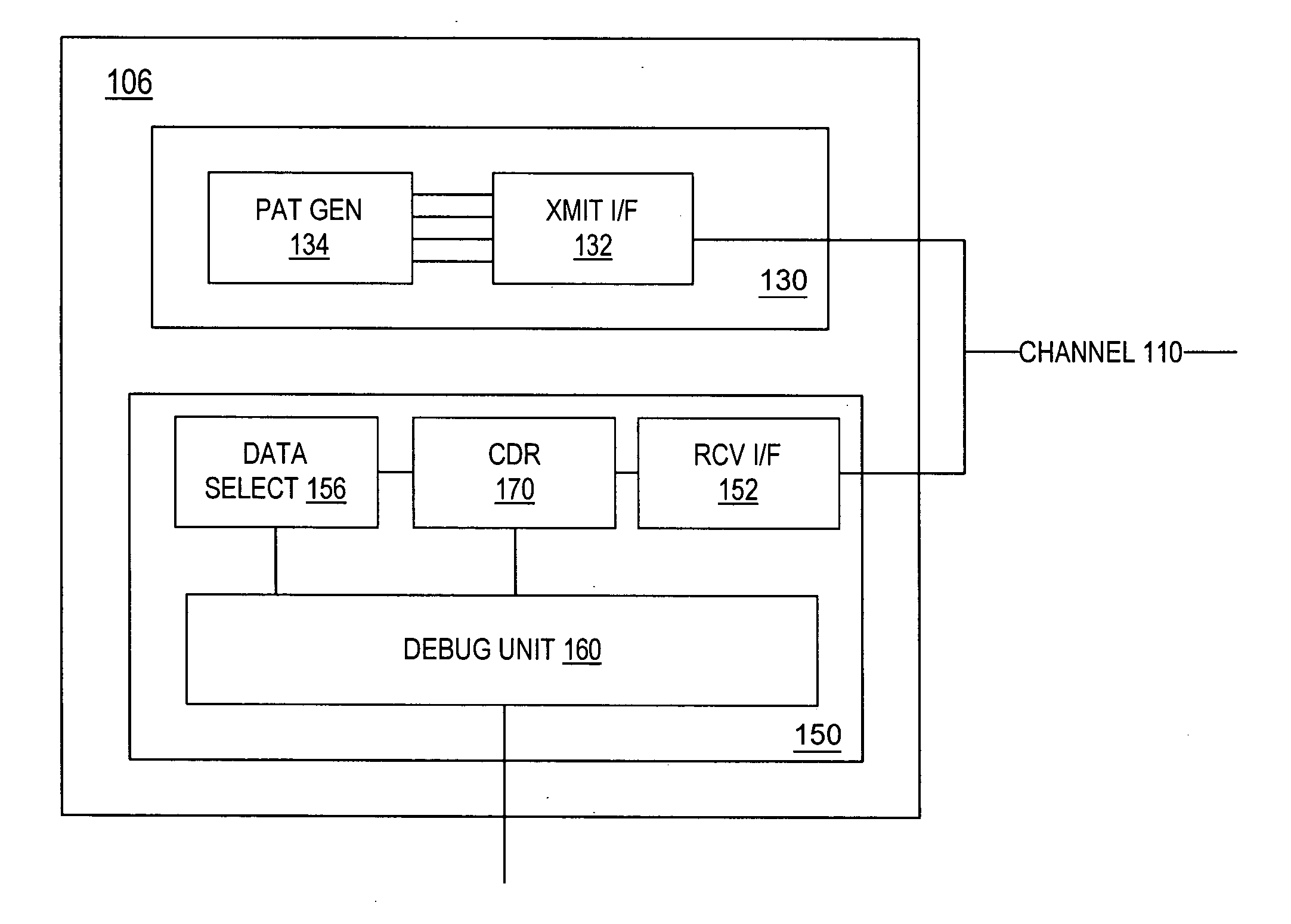
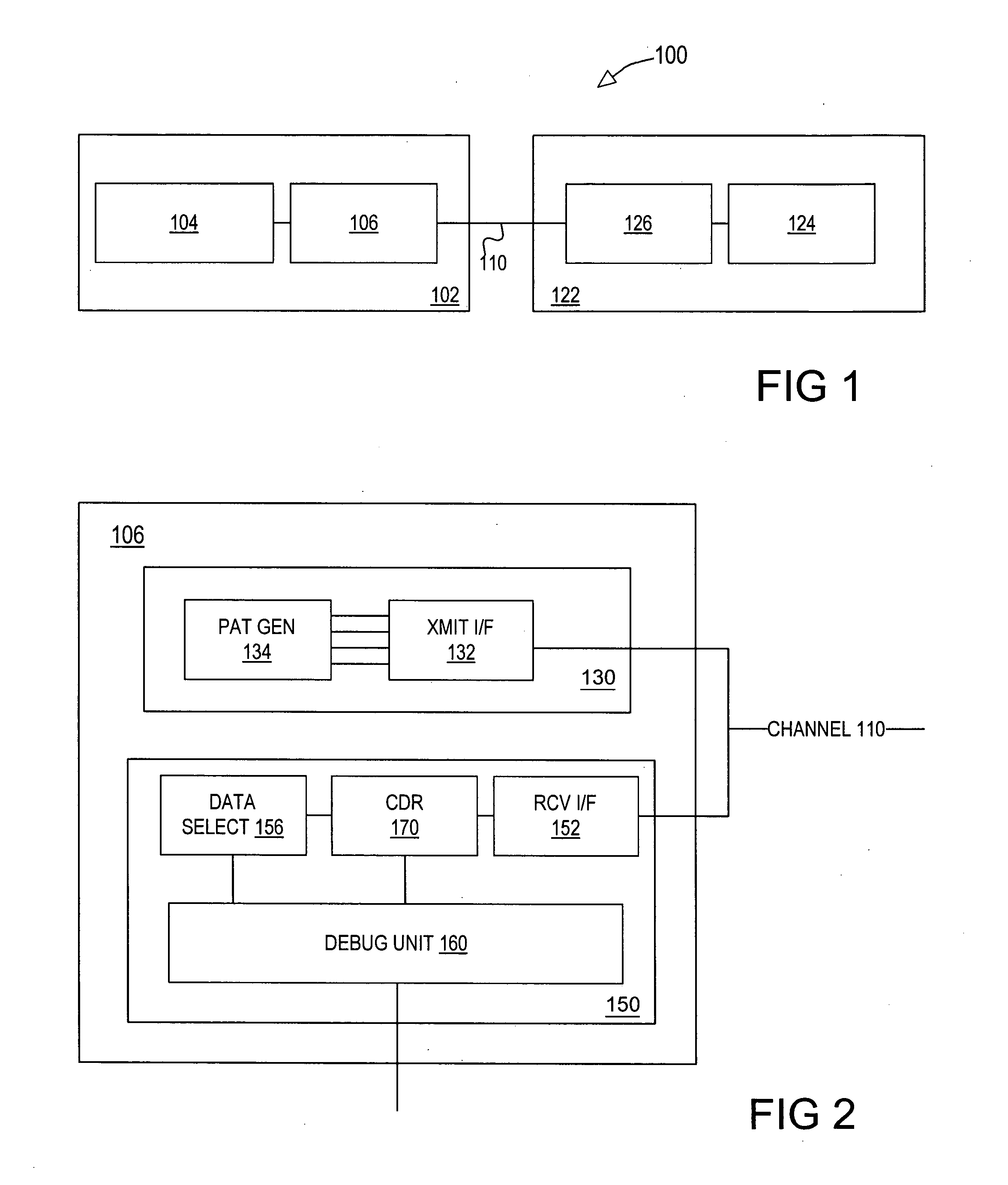
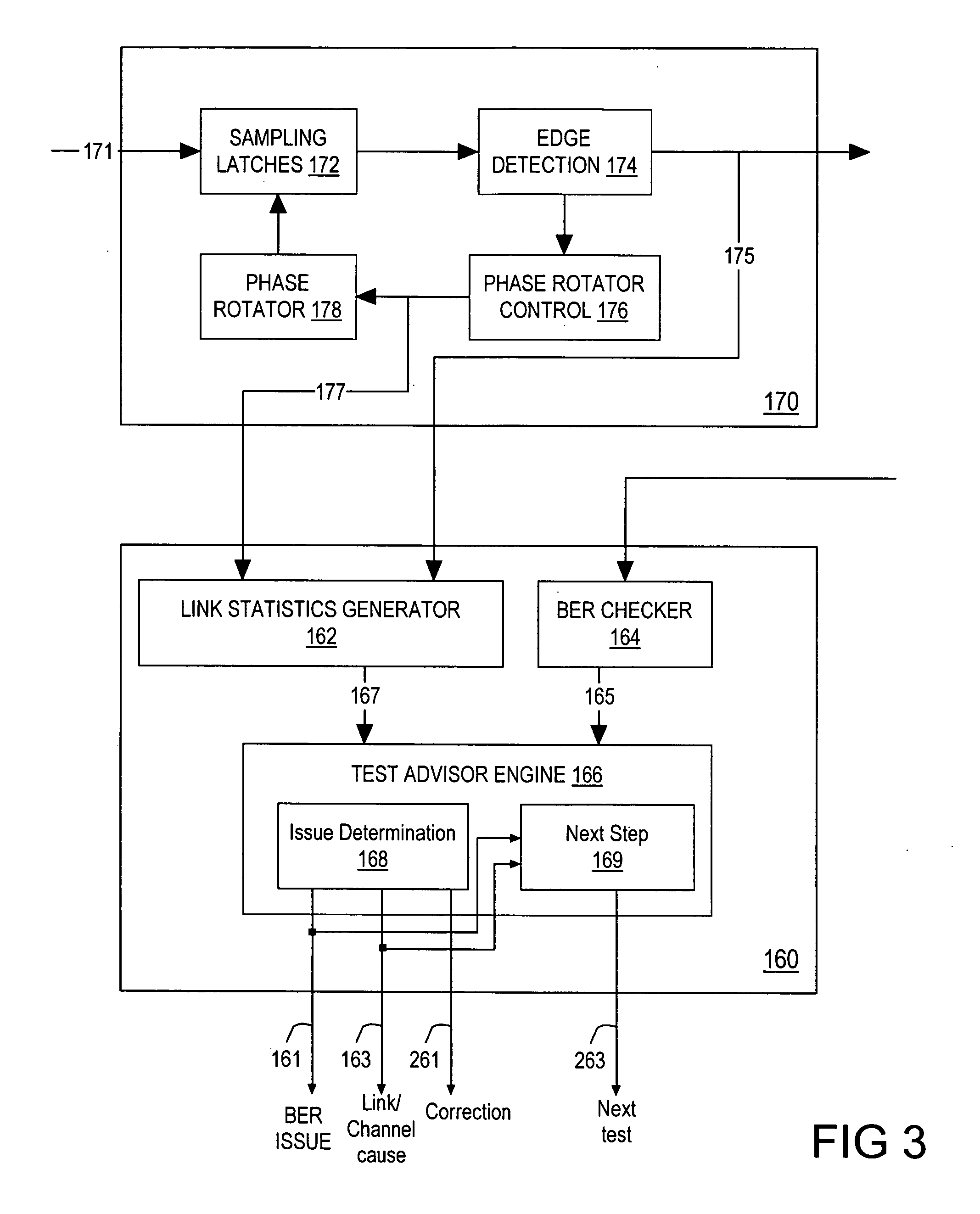
[0006] The goal identified above is achieved by a communication link for use in a data processing system according to the present invention. The communication link's receiver includes a receive interface, a clock / data recovery (CDR) circuit, and a debug unit. The receive interface receives a test signal transmitted over a communication channel and converts the voltage levels of the test signal. The CDR circuit is coupled to the receive interface and is configured to extract a clock signal and a test data signal from the received signal. A debug unit determines a bit error rate (BER) of the test data signal and at least one jitter characteristic of the signal by determining statistics associated with the CDR loop signals. The debug unit further includes a test advisor to recommend corrective action, based on the BER and the jitter characteristic(s) when the BER exceeds a predetermined threshold. The communication link further includes a transmitter having a transmit interface connected to the communication channel and a pattern generator that is connectable to the transmitter. The receive interface is preferably configured to convert non-return to zero (NRZ) formatted serial data to parallel format data with CMOS signal levels. The corrective action recommended by the debug unit can include performing at least one additional test using an additional test pattern when the BER exceeds the predetermined threshold but the jitter characteristics are acceptable. The recommended corrective action could also include modifying a characteristic of the CDR, such as the sampling rate or bandwidth, when the BER exceeds the predetermined threshold and at least one of the jitter characteristics exceeds a specified threshold. The CDR circuit includes an edge detection unit and a phase rotator control unit. An output of the edge detection unit indicative of the CDR's high frequency jitter and an output from the phase rotator control unit indicative of the CDR's frequency offset may be provided to the debug unit. In one embodiment, the debug unit employs and accesses a look up table (LUT) containing a plurality of entries, each entry having an associated BER value and at least one jitter characteristic value, to facilitate the problem determination and corrective action recommendation.

Problems solved by technology

Because of a growing number of high speed communication standards and applications, however, it is generally difficult to predict the exact application and environment in which such components will be used.
Designing to a generalized specification, such as a “bathtub curve” type of specification indicating a projected bit error rate (BER) as a function of the sampling point, is generally insufficient to guarantee an acceptable BER in any particular implementation.
Communication links, unfortunately, are generally not amenable to at-speed test and diagnosis.
Pattern-based at-speed testing using pseudo-random-bit-streams (PRBS) or similar approaches does not provide much debugging or diagnosis capability.
Direct debugging by, for example, capturing internal signals at speed is not a realistic option.
Although there has been work in detecting low-level indicators, such as jitter, this work generally requires substantial extra circuitry, and does not directly point to a system-level malfunction.

Method used


Image

  • Channel-based testing of communication link
  • Channel-based testing of communication link
  • Channel-based testing of communication link

Examples


Embodiment Construction

[0013] Generally speaking the invention contemplates a communication link of a data processing system. The link is enabled to perform on-chip, at-speed testing and analysis or diagnosis of system communication configuration, which includes the link itself as well as the communication channel in which the link is embedded. A data pattern is generated by a transmitting device to create simulated data. The simulated data and the transmitter's clock signal are serialized and transmitted over the communication channel to the link. The link's receive interface modifies the voltage levels of the received data for use with CMOS logic and provides the data to a clock / data recovery (CDR) circuitry. The CDR includes edge detection and phase correction or rotation circuitry that function to extract the clock signal from the received signal. Internal signals from the CDR are provided to a debug circuit of the receiver. A CDR loop statistics calculator in the debug circuit determines jitter stati...


PUM


Abstract

A communication link receiver for use in a data processing system includes a receive interface, a clock / data recovery (CDR) circuit, and a debug unit. The receive interface receives a test signal from the communication channel. The CDR circuit is configured to extract a clock signal and a test data signal from the received signal. A debug unit determines a bit error rate (BER) of the test data signal and at least one jitter characteristic of the communication link. The debug unit further includes a test advisor to recommend corrective action, based on the BER and the jitter characteristic(s) when the BER exceeds a predetermined threshold. The corrective action recommended can include transmitting an additional test pattern when the BER is high, but the jitter characteristics are acceptable or modifying a CDR characteristic, such as the sampling rate or bandwidth, when the BER and at least one jitter characteristic exceed their predetermined thresholds.

Description

BACKGROUND [0001] 1. Field of the Present Invention [0002] The present invention is in the field of electronic systems and more particularly in the field of high speed communication links in an electronic system. [0003] 2. History of Related Art [0004] An integrated communication link refers to the hardware system interface between two components and is composed of integrated transmitter and receiver circuits directly connected to a communication channel. Each of the components can be a general purpose processor, a memory, an application specific integrated circuit (ASIC), or another electronic device. A communication channel refers to the physical medium connecting a pair of components. Integrated communication links are found on an increasing number of integrated circuits. System-on-a-chip devices, for example, now frequently incorporate an on-board communication link enabling the device to communicate with system memory and other devices. Because of a growing number of high speed...

Claims


Application Information

Patent Timeline
IPC IPC(8): G06F11/00H04L1/20H04L1/24
CPCH04L1/205H04L1/203H04L1/24
Inventor CARBALLO, JUAN-ANTONIO
Owner IBM CORP
Learn More