Apparatus and method for an electronically tuned, wavelength-dependent optical detector

an optical detector and wavelength-dependent technology, applied in the direction of optical radiation measurement, instruments, spectrometry/spectrophotometry/monochromators, etc., can solve the problem of inability to dynamically tune the wavelength-dependent relationship, the speed with which the selected wavelength can be changed in these approaches is limited, and the msm device cannot be dynamically tuned

Inactive Publication Date: 2005-04-28
THE BOARD OF TRUSTEES OF THE LELAND STANFORD JUNIOR UNIV
View PDF11 Cites 10 Cited by
  • Summary
  • Abstract
  • Description
  • Claims
  • Application Information

AI Technical Summary

Benefits of technology

[0008] In view of the above, it is a primary object of the present invention to provide an apparatus and method for a wavelength-dependent optical detector that can be dynamically tuned over a wide range with a response time of less than a few nanoseconds. More specifically, it is an object of the present invention to provide an electronically tuned, wavelength-dependent optical detector.
[0009] These and numerous other objects and advantages of the present invention will become apparent upon reading the following description.
[0010] The objects and advantages of the present invention are secured by an apparatus and method for an electronically tuned, wavelength-dependent optical detector. The electronically tuned, wavelength-dependent optical detector is a modified MSM photodetector. In the modified MSM device, a comb-like metal electrode, comprising at least five, substantially parallel arms with a fixed spacing from each other and having a common voltage, is deposited on a surface of a semiconductor. At least four metal electrodes, interdigitated with the comb-like metal electrode are also deposited on the surface of the semiconductor. Each of the metal electrodes is connected to a voltage means that applies a control voltage to each metal electrode. By applying a set of control voltages to the metal electrodes using the voltage means, a wavelength to be detected in a stream of light illuminating the modified MSM device is selected.
[0011] In one embodiment of the invention, the comb-like metal electrode in the modified MSM device is connected to an amplifier.
[0012] In another embodiment, an opaque coating is deposited on parts of the surface of the modified MSM device thereby grouping the arms of the comb-like metal electrode and the metal electrodes into pairs.
[0013] In another embodiment, the semiconductor in the modified MSM device is selected based on the wavelengths to be detected. GaAs is used for MSM devices in the 800 nm wavelength range. InAlAs deposited on InGaAs is used for MSM devices in the 1600 nm wavelength range.

Problems solved by technology

While such MSM devices have been successfully employed in a variety of applications, a principal limitation of the MSM device is that the wavelength-dependence cannot be dynamically tuned.
However, the speed with which the selected wavelength can be changed in these approaches is limited when the dynamic tuning is based on mechanical motion, such as that associated with a stepper motor or thermal expansion.
A PIN detector with multiple quantum wells can be dynamically tuned with a fast response time; however, such devices only have a coarse tuning capability over a small range of wavelengths and require a large biasing voltage.
These limitations in the dynamic tuning of the wavelength dependence of existing optical detectors are particularly problematic in existing or proposed optical communications systems based on Wavelength Division Multiplexing (WDM).
The alternative, involving a plurality of wavelength-dependent optical detectors with slow dynamic tuning response times, would be expensive and difficult to manufacture and maintain.

Method used


Image

  • Apparatus and method for an electronically tuned, wavelength-dependent optical detector
  • Apparatus and method for an electronically tuned, wavelength-dependent optical detector
  • Apparatus and method for an electronically tuned, wavelength-dependent optical detector

Examples


Embodiment Construction

and the preferred and alternative embodiments is presented below in reference to the attached drawing figures.

BRIEF DESCRIPTION OF THE FIGURES

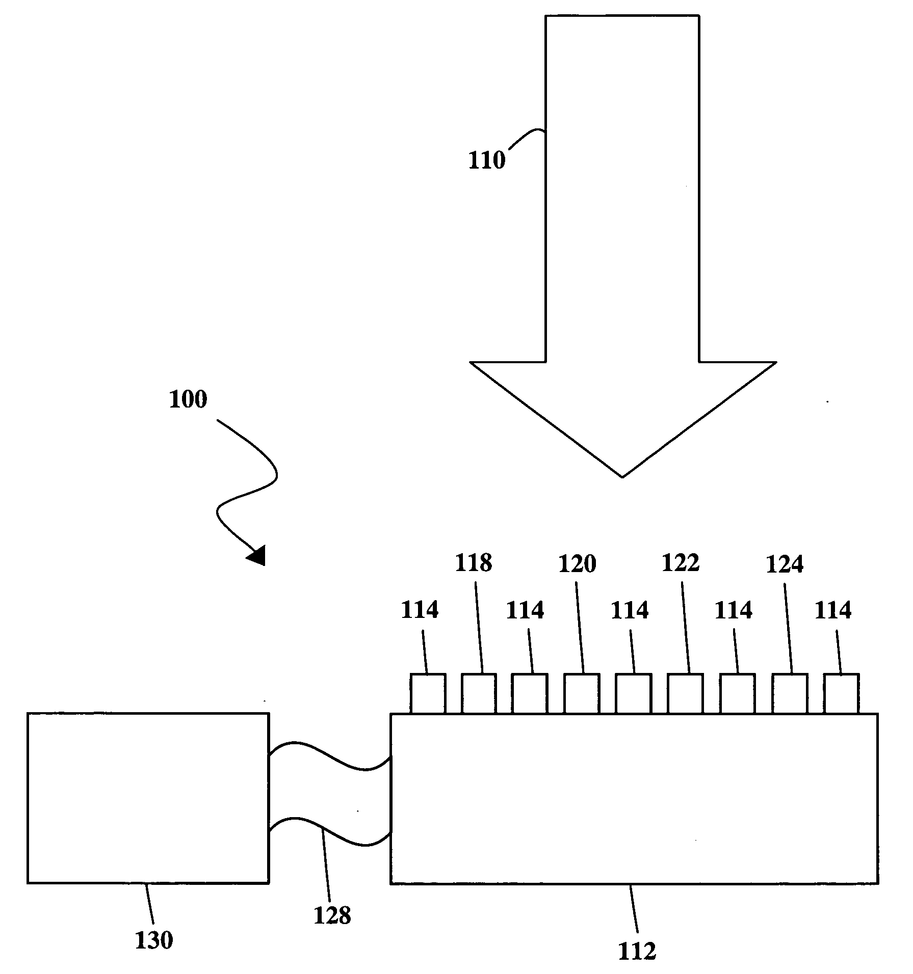
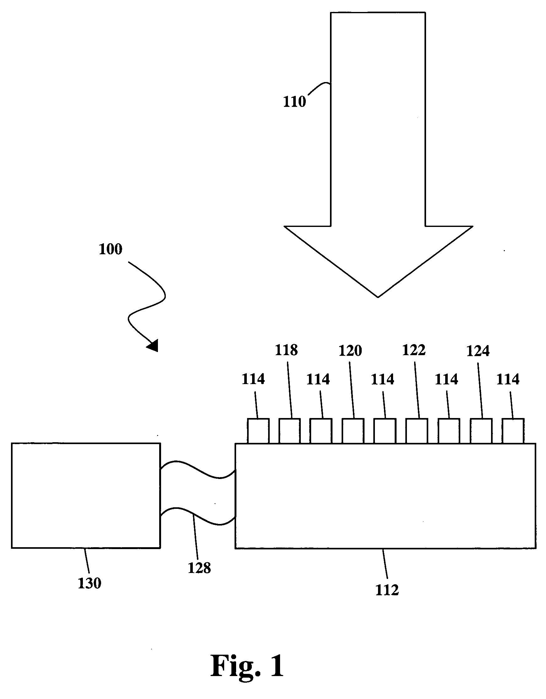
[0020]FIG. 1 is a diagram illustrating a side view of an apparatus according to the invention.

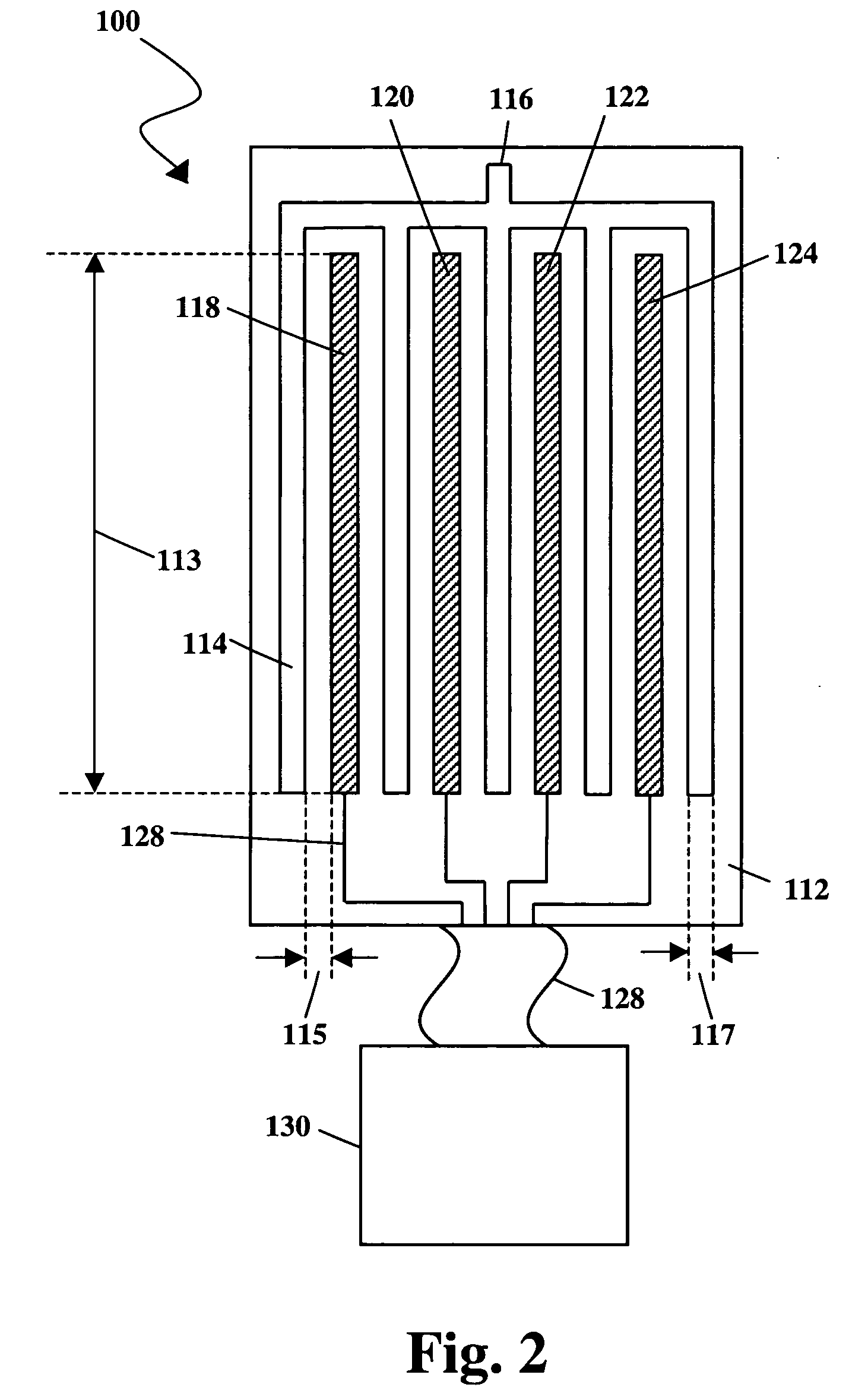
[0021]FIG. 2 is a diagram illustrating a top view of an apparatus according to the invention.

[0022]FIG. 3 is a diagram illustrating a top view of another embodiment of an apparatus according to the invention.

[0023]FIG. 4 is a diagram illustrating a side view of another embodiment of an apparatus according to the invention.

[0024]FIG. 5 is a diagram illustrating an optical system incorporating an apparatus according to the invention.

[0025]FIG. 6 is a diagram illustrating an experimental set-up.

[0026]FIG. 7 is a diagram showing the measured photocurrent as a function of wavelength.

[0027]FIG. 8 is a diagram illustrating a biasing configuration relative to the fringes of an interference pattern for an apparatus according to the invention.

[0028]FIG...


PUM


Abstract

An apparatus and method for an electronically tuned, wavelength-dependent optical detector are disclosed. The electronically tuned, wavelength-dependent optical detector is a modified metal-semiconductor-metal photodetector comprising a comb-like metal electrode at a common voltage and metal electrodes each supplied with a control voltage by a voltage means. The wavelength to be detected in a stream of light illuminating the electronically tuned, wavelength-dependent optical detector is selected based on the set of control voltages applied to the metal electrodes using the voltage means and the relative position of the electronically tuned, wavelength-dependent optical detector. In another embodiment of the invention, the wavelength to be detected with the electronically tuned, wavelength-dependent optical detector is also selected using a standing wave generator, such as an interferometer, to produce a spatially varying light intensity on the surface of the electronically tuned, wavelength-dependent optical detector.

Description

FIELD OF THE INVENTION [0001] The present invention relates generally to an apparatus and method for an electronically tuned, wavelength-dependent optical detector. BACKGROUND OF THE INVENTION [0002] Wavelength-dependent optical detectors are essential optical components that are incorporated in a myriad of applications including spectrometers, optical interconnects and optical communications systems. [0003] An existing wavelength-dependent optical detector is the so-called metal-semiconductor-metal (MSM) photodetector. In this device, an interdigitated pair of metal electrodes is deposited on a surface of a semiconductor. Light illuminating the MSM device is absorbed in the semiconductor producing charge carriers that drift to the neighboring metal electrodes when a voltage is applied to the metal electrodes. The resulting light-induced current is amplified and detected by an amplifier. The wavelength-dependence of the MSM device is partially determined by the absorption characteri...

Claims


Application Information

Patent Timeline
Patent Type & Authority Applications(United States)
IPC IPC(8): H01J40/14H01L31/00
CPCG01J3/32H01L31/1085G01J3/453
Inventor CHEN, RAYMILLER, DAVID A.B.
Owner THE BOARD OF TRUSTEES OF THE LELAND STANFORD JUNIOR UNIV
Why Eureka
Try Eureka