Magnetic random access memory cell

a random access and memory cell technology, applied in the field of memory devices, can solve the problems of not significantly increasing the cost of manufacturing the improved magnetic memory cell, and achieve the effects of reducing the lateral size of the associated mtj device, increasing the cell density, and reducing the total magnetic moment of the memory cell

Active Publication Date: 2005-04-28
IBM CORP
View PDF2 Cites 39 Cited by
  • Summary
  • Abstract
  • Description
  • Claims
  • Application Information

AI Technical Summary

Benefits of technology

[0005] The present invention is an improved magnetic memory cell including an n-transistor, n-MTJ (nTnMTJ) architecture providing increased cell density without significantly reducing a lateral size of the MTJ device associated with the memory cell, and therefore without significantly reducing a total magnetic moment of the memory cell. Since the total magnetic moment of the memory cell can be maintained, the cell does not suffer from spontaneous switching which can undesirably affect the data integrity of the memory cell. Moreover, the memory cell architecture of the present invention may be formed using a conventional integrated circuit (IC) fabrication technology, such as, for example, a CMOS process. Consequently, the cost of manufacturing the improved magnetic memory cell is not significantly increased.

Problems solved by technology

Consequently, the cost of manufacturing the improved magnetic memory cell is not significantly increased.

Method used


Image

  • Magnetic random access memory cell
  • Magnetic random access memory cell
  • Magnetic random access memory cell

Examples


Embodiment Construction

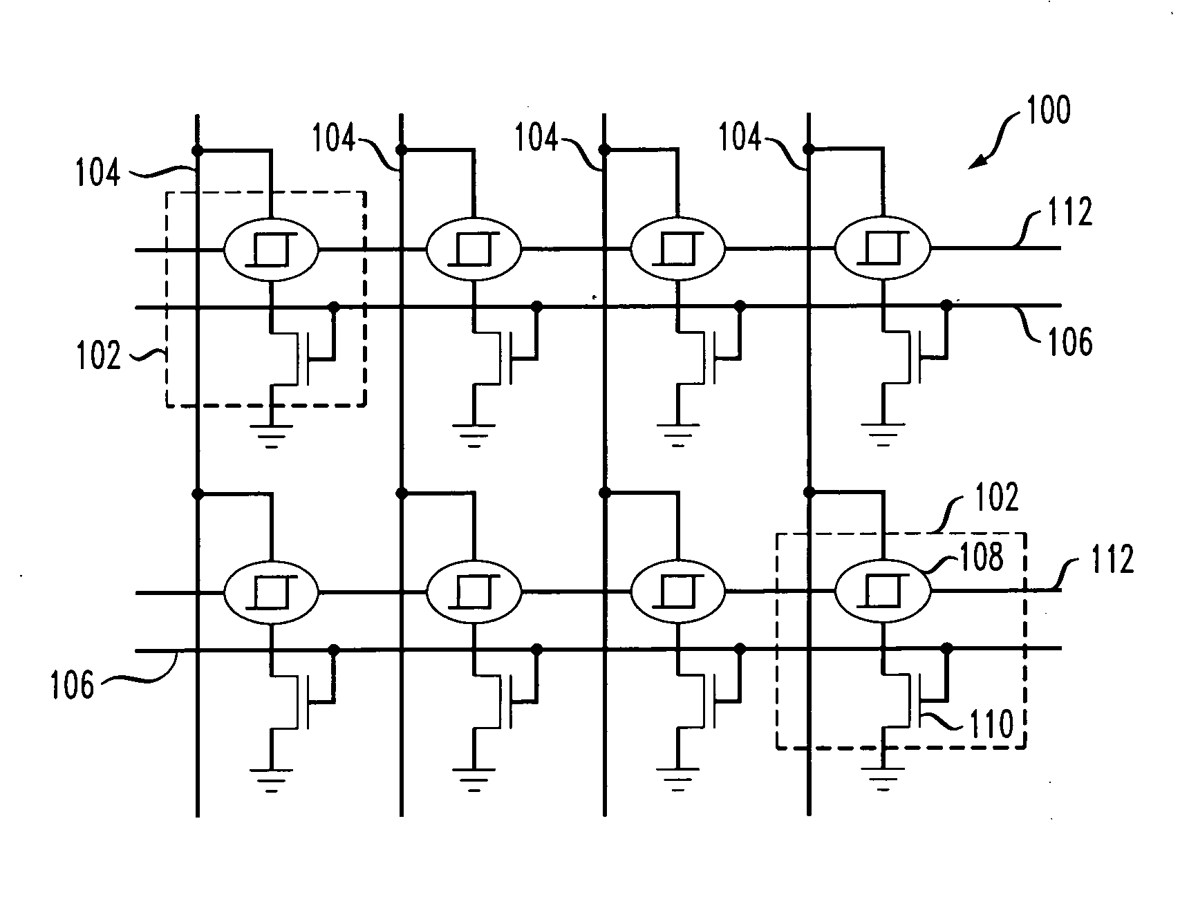
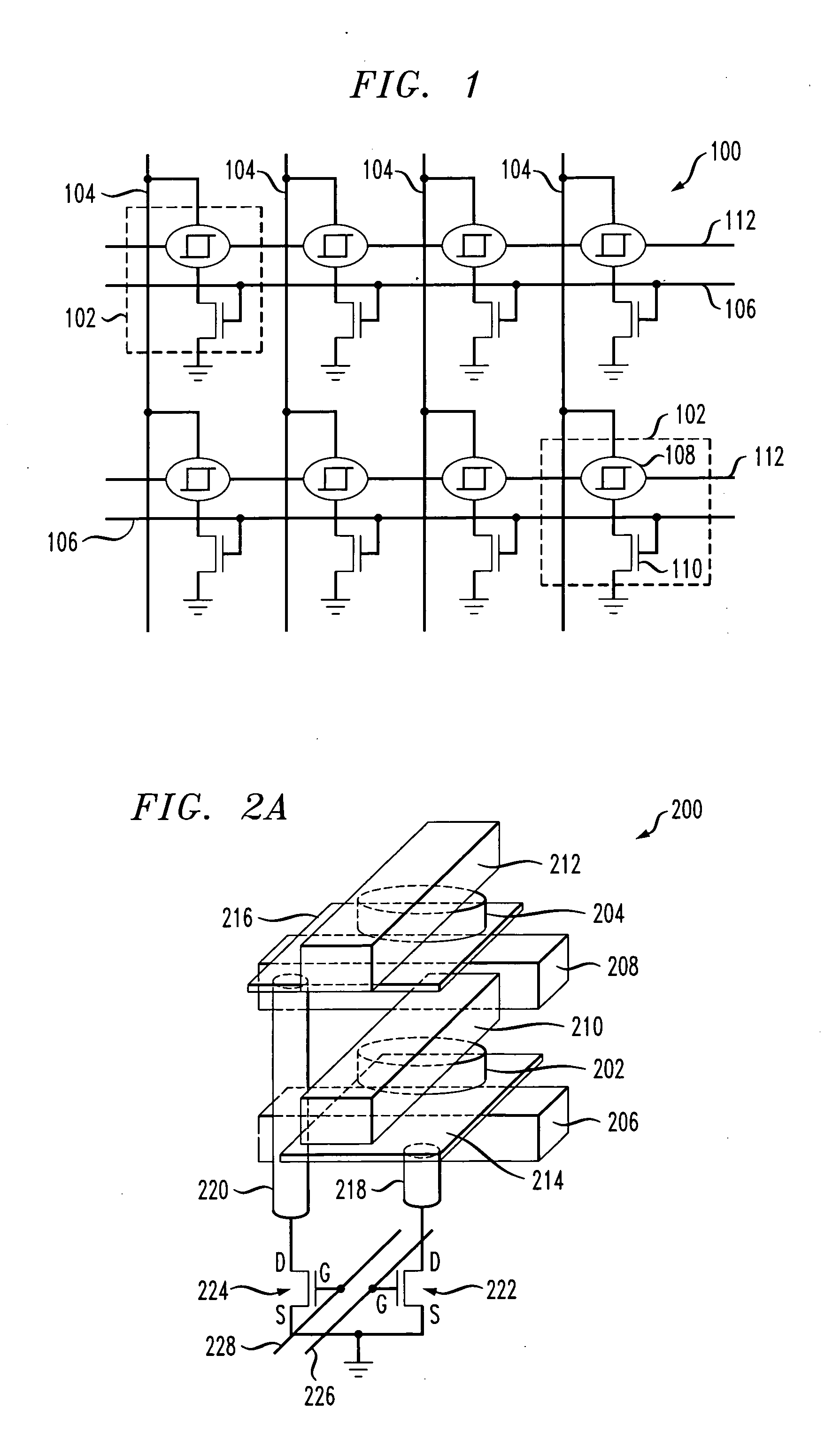
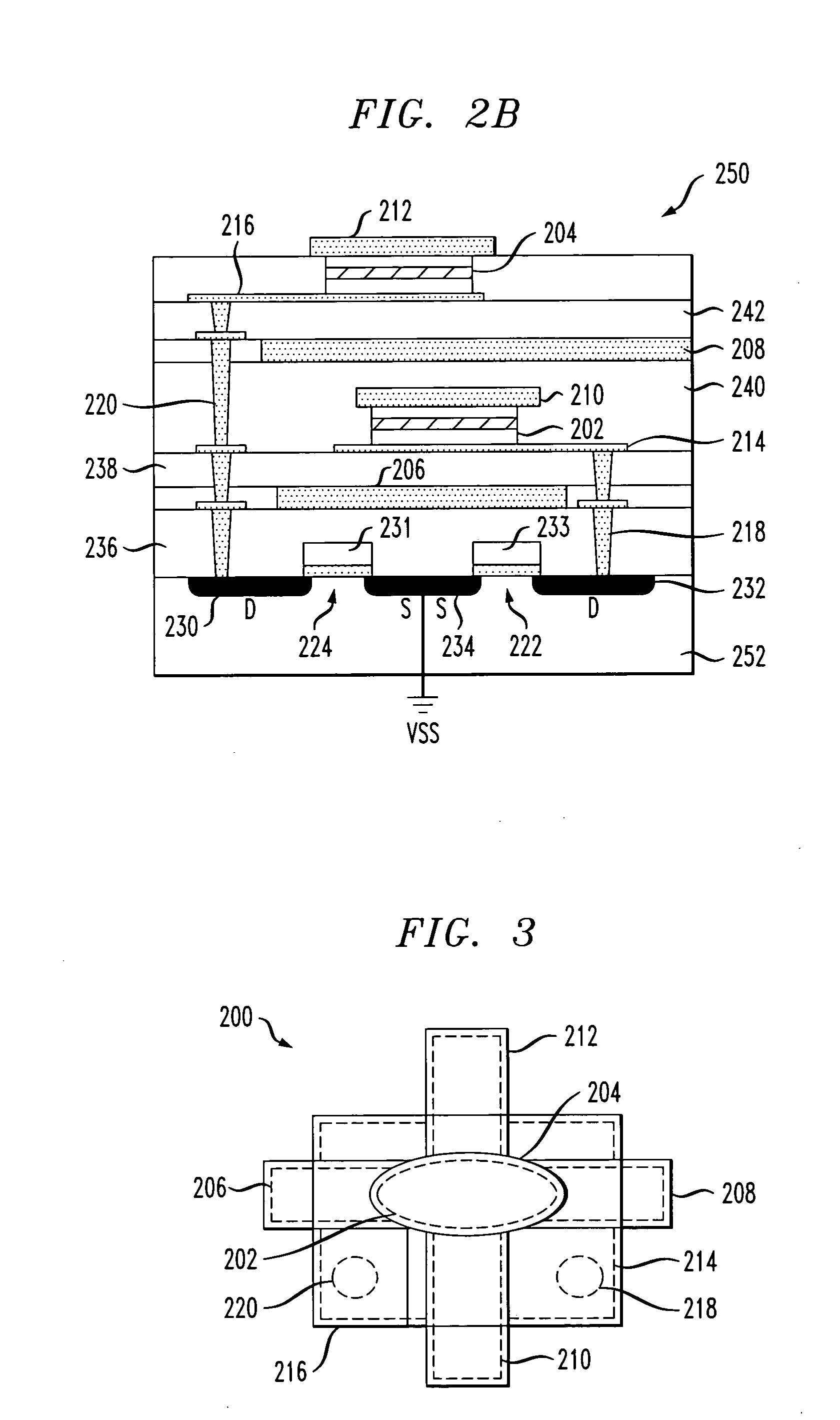
[0012] The present invention will be described herein in the context of an illustrative magnetic memory cell which may be used in an MRAM. It should be appreciated, however, that the invention is not limited to this or any particular memory cell architecture. Rather, the invention is more generally applicable to techniques for advantageously increasing a density of the magnetic memory cell without also reducing a lateral size of the magnetic storage element(s) associated with the cell. Since the total magnetic moment of the memory cell is directly related to the lateral size of the corresponding storage element, the total magnetic moment of the memory cell is beneficially maintained. Moreover, although implementations of the present invention are described herein with reference to metal-oxide-semiconductor (MOS) transistors and MTJ devices, it should be appreciated that the invention is not limited to such devices, and that alternative devices, such as, for example, bipolar junction...


PUM


Abstract

A memory cell for use in a magnetic random access memory (MRAM) circuit includes at least first and second transistors formed in a semiconductor layer. A first insulating layer is formed on at least a portion of the first and second transistors. The memory cell further includes a first magnetic storage element formed on at least a portion of the first insulating layer, at least a second insulating layer formed on at least a portion of the first magnetic storage element, and at least a second magnetic storage element formed on at least a portion of the second insulating layer. The first and second magnetic storage elements are electrically connected to the first and second transistors, respectively.

Description

FIELD OF THE INVENTION [0001] The present invention relates generally to memory devices, and more particularly relates to a magnetic random access memory (MRAM) cell architecture having an increased density. BACKGROUND OF THE INVENTION [0002] An MRAM cell typically includes a magnetic storage element, for example, a magnetic tunnel junction (MTJ) device, for storing a bit of information represented by two stable states in which the memory cell can reside. While semiconductor process technology, such as, for example, complementary metal-oxide-semiconductor (CMOS) technology, used to fabricate MRAM cells continues to scale aggressively below 0.18 micron (μm) dimensions, conventional MTJ devices often encounter difficulties due at least in part to a super-paramagnetic effect. The super-paramagnetic effect generally arises from the basic principles of thermal dynamics and is related to the total magnetic moment per bit, the switching field, and the temperature of the MTJ device in stora...

Claims


Application Information

Patent Timeline
Patent Type & Authority Applications(United States)
IPC IPC(8): G11C11/16H01L21/8246H01L27/22H01L29/76
CPCB82Y10/00H01L27/228G11C11/16H10B61/22
Inventor LU, YU
Owner IBM CORP
Why Eureka
Try Eureka