Flip-chip light emitting diode

a light-emitting diode and flip-chip technology, applied in the field of electronic arts, can solve the problems of difficult simultaneous optimization of optical, electrical and thermal properties of the electrode, inability to tune the electrode reflectivity, and low metal electrode reflectivity in finished devices

Inactive Publication Date: 2005-04-28
GELCORE LLC (US)
View PDF11 Cites 145 Cited by
  • Summary
  • Abstract
  • Description
  • Claims
  • Application Information

AI Technical Summary

Problems solved by technology

The multitasking of the electrodes presents design problems, as it may be difficult to simultaneously optimize optical, electrical, and thermal properties of the electrodes.
Metal electrode reflectivity in finished devices

Method used


Image

  • Flip-chip light emitting diode
  • Flip-chip light emitting diode
  • Flip-chip light emitting diode

Examples


Embodiment Construction

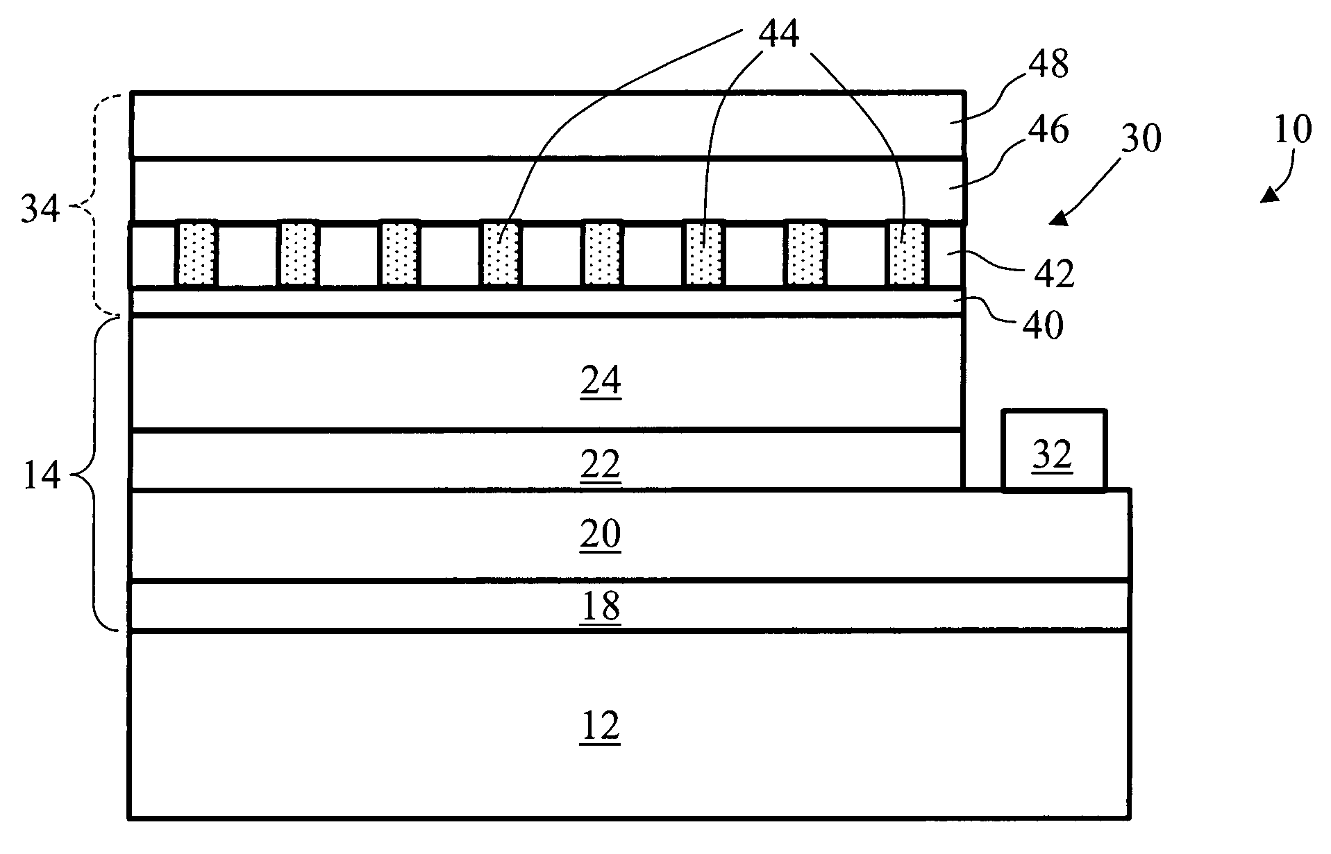
[0017] With reference to FIG. 1, a flip-chip light emitting diode device 10 includes a light-transmissive substrate 12 with a plurality of semiconductor layers 14 deposited thereon. In a preferred embodiment, the substrate is sapphire, ZnO, lithium gallate, AlN, AlxInyGa1-y-xN, or silicon carbide (SiC), and the semiconductor layers 14 are selected group III-nitride layers such as GaN layers, AlN layers, InN layers, and ternary and quaternary alloys thereof.

[0018] The semiconductor layers 14 are preferably formed on the light-transmissive substrate 12 by metalorganic chemical vapor deposition (also known in the art as organometallic vapor phase epitaxy and similar nomenclatures), molecular beam epitaxy, chemical beam epitaxy, or another epitaxial film deposition technique. However, light emitting diodes of other material systems, such as the group III-phosphides, group III-arsenides, and group IV semiconductors, can also be used. If no suitable light transmissive substrate for epita...


PUM


Abstract

A flip chip light emitting diode die (10, 10′, 10″) includes a light-transmissive substrate (12, 12′, 12″) and semiconductor layers (14, 14′, 14″) that are selectively patterned to define a device mesa (30, 30′, 30″). A reflective electrode (34, 34′, 34″) is disposed on the device mesa (30, 30′, 30″). The reflective electrode (34, 34′, 34″) includes a light-transmissive insulating grid (42, 42′, 60, 80) disposed over the device mesa (30, 30′, 30″), an ohmic material (44, 44′, 44″, 62) disposed at openings of the insulating grid (42, 42′, 60, 80) and making ohmic contact with the device mesa (30, 30′, 30″), and an electrically conductive reflective film (46, 46′, 46″) disposed over the insulating grid (42, 42′, 60, 80) and the ohmic material (44, 44′, 44″, 62). The electrically conductive reflective film (46, 46′, 46″) electrically communicates with the ohmic material (44, 44′, 44″, 62).

Description

BACKGROUND [0001] The present invention relates to the electronics arts. It especially relates to flip-chip group III-nitride light emitting diodes for lighting applications, and will be described with particular reference thereto. However, the invention also finds application in conjunction with other types of flip-chip light emitting diodes, and in other optoelectronic devices. [0002] In the flip-chip mounting configuration, a light emitting diode with a light-transmissive substrate and front-side electrodes is bonded “face down” to a substrate. For example, a gallium nitride-based light emitting diode that includes active gallium nitride-based layers grown on a transparent sapphire or silicon carbide substrate can be flip-chip bonded. The flip-chip mounting configuration has a number of advantages, including improved thermal heat sinking due to a close proximity of the front-side active layers to the heat sinking substrate, and elimination of shadowing losses due to the contacts....

Claims


Application Information

Patent Timeline
IPC IPC(8): H01L23/48H01L33/38H01L33/40
CPCH01L33/387H01L2933/0083H01L33/405
Inventor STOKES, EDWARD B.D'EVELYN, MARK P.WEAVER, STANTON E.SANDVIK, PETER M.EBONG, ABASIFREKE U.CAO, XIAN-ANLEBOEUF, STEVEN F.TASKAR, NIKHIL R.
Owner GELCORE LLC (US)
Why Eureka
Try Eureka