Passive alignment of VCSELs to waveguides in opto-electronic cards and printed circuit boards

a technology of optoelectronic cards and printed circuit boards, applied in the direction of optical waveguide light guides, instruments, optical elements, etc., can solve the problems of adversely affecting the reliability and service life of the entire electronic package, and achieve the effects of improving the thermal stability of the applicable optoelectronic card or printed circuit board, enhancing versatility and economic efficacy, and improving passive alignmen

Inactive Publication Date: 2005-04-28
IBM CORP
View PDF12 Cites 34 Cited by
  • Summary
  • Abstract
  • Description
  • Claims
  • Application Information

AI Technical Summary

Benefits of technology

[0021] Accordingly, in order to obviate or ameliorate any drawbacks encountered in the prior art, the present invention is directed to the obtaining of an improved passive alignment between VCSELs or PIN arrays and waveguides within electronic built-up layers of opto-electronic packages. Moreover, the thermal stability of the applicable opto-electronic card or printed circuit board (PCB) may be considerably improved through the employment of a core constituted of a low expansion material mounting the optical components and a first built-up layer, as a consequence of which the accommodation of larger VCSELs and PIN arrays, as well as the use of smaller waveguide dimensions can be readily rendered possible so as to enhance the versatility and economic efficacy of the present invention.
[0023] Pursuant to one aspect of the invention, the extent of precision of alignment between the VCSEL, the PIN arrays and the mirrors of the waveguide may be readily controlled by simultaneously etching a second cladding or organic layer located on a core or substrate so as to form the waveguide channels and the C4 openings. The C4 openings expose a portion of each pad which is to be electrically connected to the transmitter or receiver chips, in view of which the exact position of the C4s is determined not by the pad but rather by the opening in the second cladding or organic layer printed on the surface of the core. This may be termed a so-called “mask-defined” C4 in its differentiation from a “pad-defined” C4 where the solder joint wets the entire pad. The foregoing may be followed by plating the electronic circuits, filling the channels with waveguide material, and then adding the upper cladding or organic layer. Inasmuch as the mirrors in the waveguide channel and the openings leading to the C4 pads are formed simultaneously, they can be positioned in an extremely precise relationship relative to each other, and at very low and acceptable tolerances.

Problems solved by technology

As a result of this type of arrangement, tolerances accumulate through the various manufacturing steps so as to collectively cause misalignment among the various components, which may adversely affect the reliability and service life of the entire electronic package.

Method used


Image

  • Passive alignment of VCSELs to waveguides in opto-electronic cards and printed circuit boards
  • Passive alignment of VCSELs to waveguides in opto-electronic cards and printed circuit boards
  • Passive alignment of VCSELs to waveguides in opto-electronic cards and printed circuit boards

Examples


Embodiment Construction

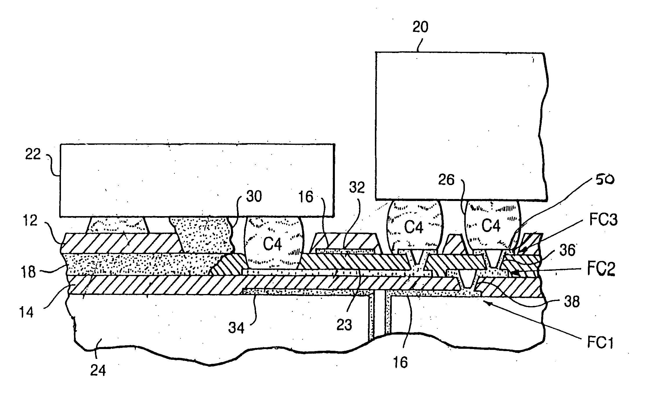
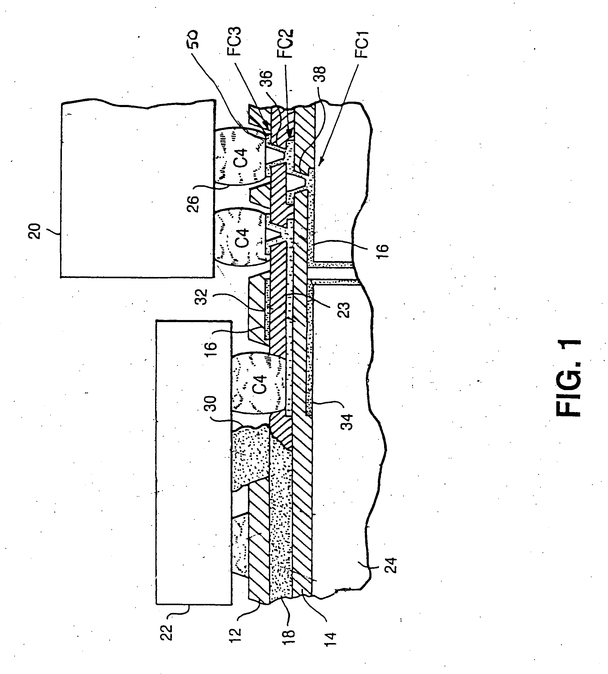
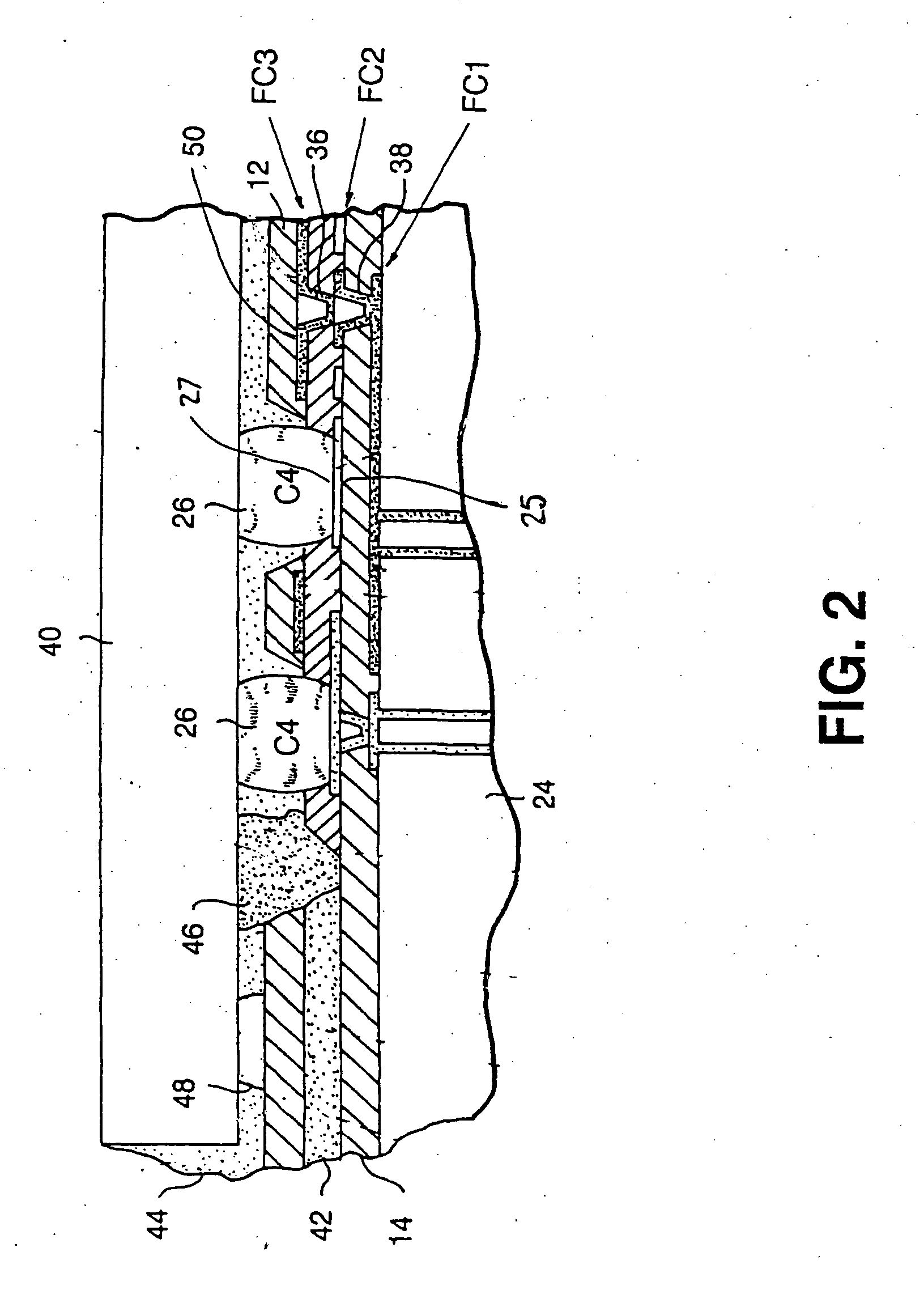
[0029] Referring specifically to FIG. 1 of the drawings, there is illustrated a sectional view of a portion of an inventive structure with two built-up cladding layers 12, 14 for wiring 16 and discrete transmitter / receiver waveguide 18 in an intermediate layer, including a signal plane 23, and processor chips 20; and an optical device 22. Additional wiring layers can be added above the upper cladding layer 12, however, thermal stability and electrical performance are at their optimum with the present structure.

[0030] The foregoing structural configuration eliminates the need for a solder mask inasmuch as the upper cladding layer 12 can readily serve for this purpose. The core 24 can be comprised of any low expansion material which approaches the coefficient of thermal expansion (CTE) of the chips 20, thereby further improving alignment and minimizing any encountered strain in the C4 joints 26. Hereby, standard epoxy glass composites can be employed for the core, consisting of cloth...


PUM


Abstract

A method of producing opto-electronic cards and printed circuit boards which are adapted to provide for passive alignment of VCSELs to waveguides. Also provided are opto-electronic cards and printed circuit boards which incorporate structure providing for the passive alignment of VCSELs to waveguides.

Description

BACKGROUND OF THE INVENTION [0001] 1. Field of the Invention [0002] The present invention relates to a method of producing opto-electronic cards and printed circuit boards which are adapted to provide for the passive alignment of VCSELs to waveguides. Moreover, the invention relates to opto-electronic cards and printed circuit boards which incorporate structure providing for the passive alignment of VCSELs to waveguides. [0003] Basically, optical waveguides operate with higher ranges of bandwidths than copper circuits which are employed in printed circuit boards, consequently requiring essentially less operating power, while also not being as susceptible to so-called cross-talk which is encountered in such types of printed circuit boards. Ordinarily, in the technology, waveguides have been utilized in connection with transmissions taking place over long distances; however, more recently, as a result of decreasing manufacturing costs and due to the high bandwidths which are achievabl...

Claims


Application Information

Patent Timeline
Patent Type & Authority Applications(United States)
IPC IPC(8): G02B6/12G02B6/122G02B6/42
CPCG02B6/12004G02B6/1221G02B2006/12176G02B6/4232G02B2006/12104G02B6/42H01L2224/16225
Inventor JOHNSON, ERIC A.CALETKA, DAVID V.
Owner IBM CORP
Why Eureka
Try Eureka