Card manufacturing technique and resulting card

a card manufacturing and card manufacturing technology, applied in the field of circuit boards, can solve the problems of high risk of electrostatic discharge, low esd protection for susceptible easy entry and damage of electrostatic discharge to circuit components of memory cards, so as to avoid damage to other circuit components from high voltage discharge, short circuit, and less prone to short circuiting of multiple conductive layers

Inactive Publication Date: 2005-04-28
SANDISK TECH LLC
View PDF4 Cites 15 Cited by
  • Summary
  • Abstract
  • Description
  • Claims
  • Application Information

AI Technical Summary

Benefits of technology

[0006] Memory cards are getting smaller and thinner, yet the capacity is increasing and they are also becoming more densely packaged. Frequent handling of these cards results in a high risk of electrostatic discharge (ESD).
[0008] During the manufacturing of the memory card, the circuit board is trimmed to its final dimensions. Conductive segments of a metallic layer that are located at the edge of the circuit board are deformed during the trimming process and can extend over an insulating layer and contact a second metallic layer, in this case either the ground or power layer, thus resulting a short circuit. As previously mentioned, it is desirous to extend the ground and / or power layer to the junction of the card for electrostatic discharge purposes. Therefore, in order to avoid short circuiting yet preserve maximum ESD protection, small gaps are formed at the edge of the second conductive layer that are vertically aligned with the conductive segments such that any deformation that may occur during the trimming process will not result in a short circuit. The deformation of the conductive segments will fall into the gap at the edge of the second conductive layer rather than making contact with the layer. The size of the gaps is small in relation to the remaining edge of the ground and / or power layer at the junction of the circuit board and the cover, thus ensuring a high level of ESD protection while avoiding short circuits from the trimming of the board.

Problems solved by technology

Frequent handling of these cards results in a high risk of electrostatic discharge (ESD).
At a junction between the plastic cover and an edge of the circuit board there is a gap where an electrostatic discharge is prone to enter and damage the circuit components of the memory card.
A prior method of avoiding short circuits due to the trimming process involved pulling back the entire edge of the conductive layer away from the edge of the circuit board, however this method affords little if any ESD protection to the susceptible components of the memory card.
Conductive segments of a metallic layer that are located at the edge of the circuit board are deformed during the trimming process and can extend over an insulating layer and contact a second metallic layer, in this case either the ground or power layer, thus resulting a short circuit.

Method used


Image

  • Card manufacturing technique and resulting card
  • Card manufacturing technique and resulting card
  • Card manufacturing technique and resulting card

Examples


Embodiment Construction

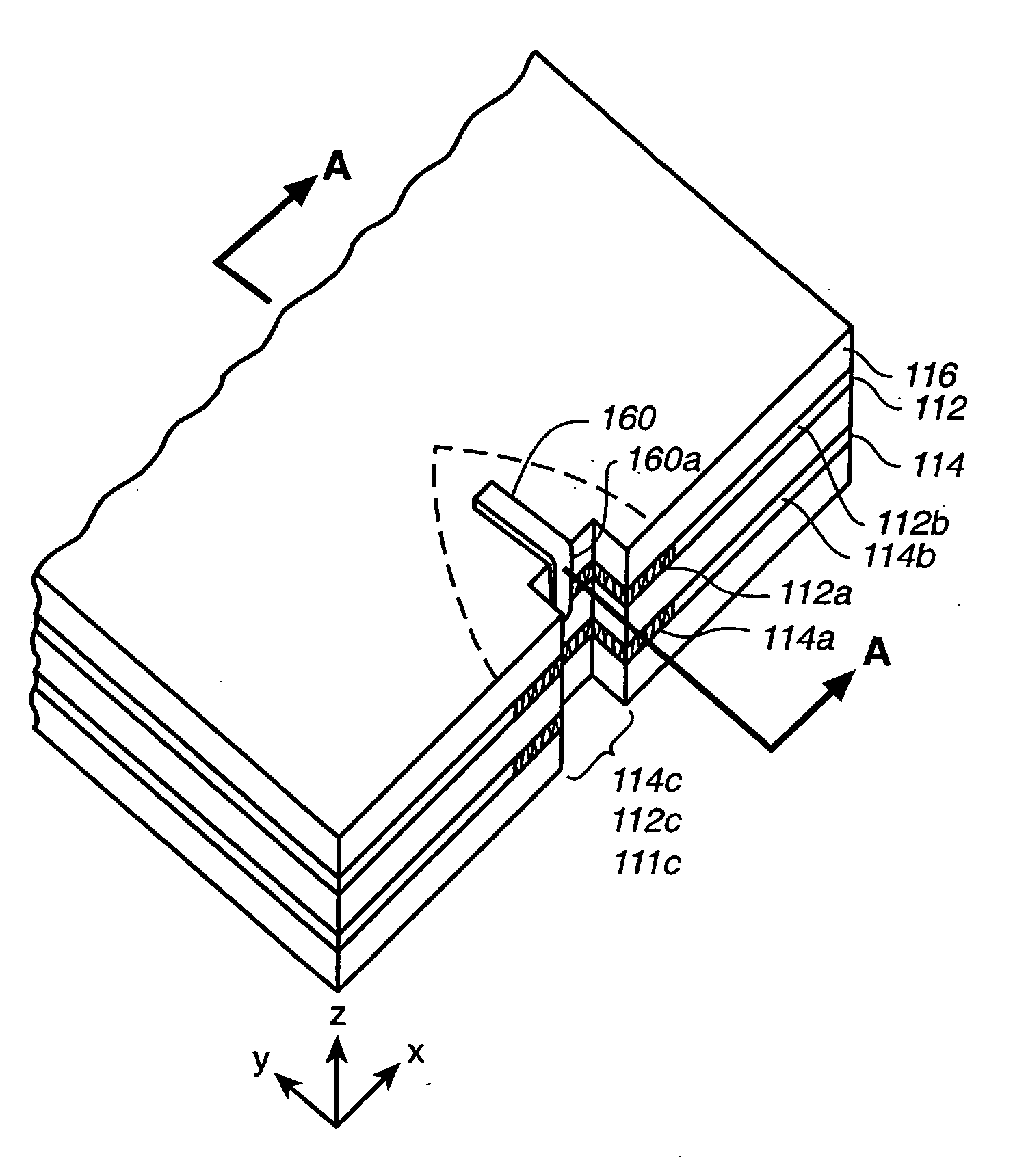
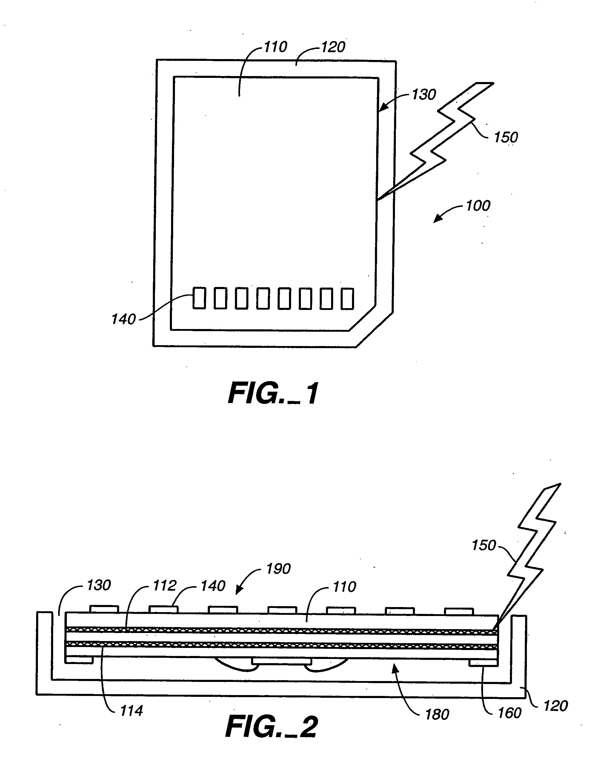
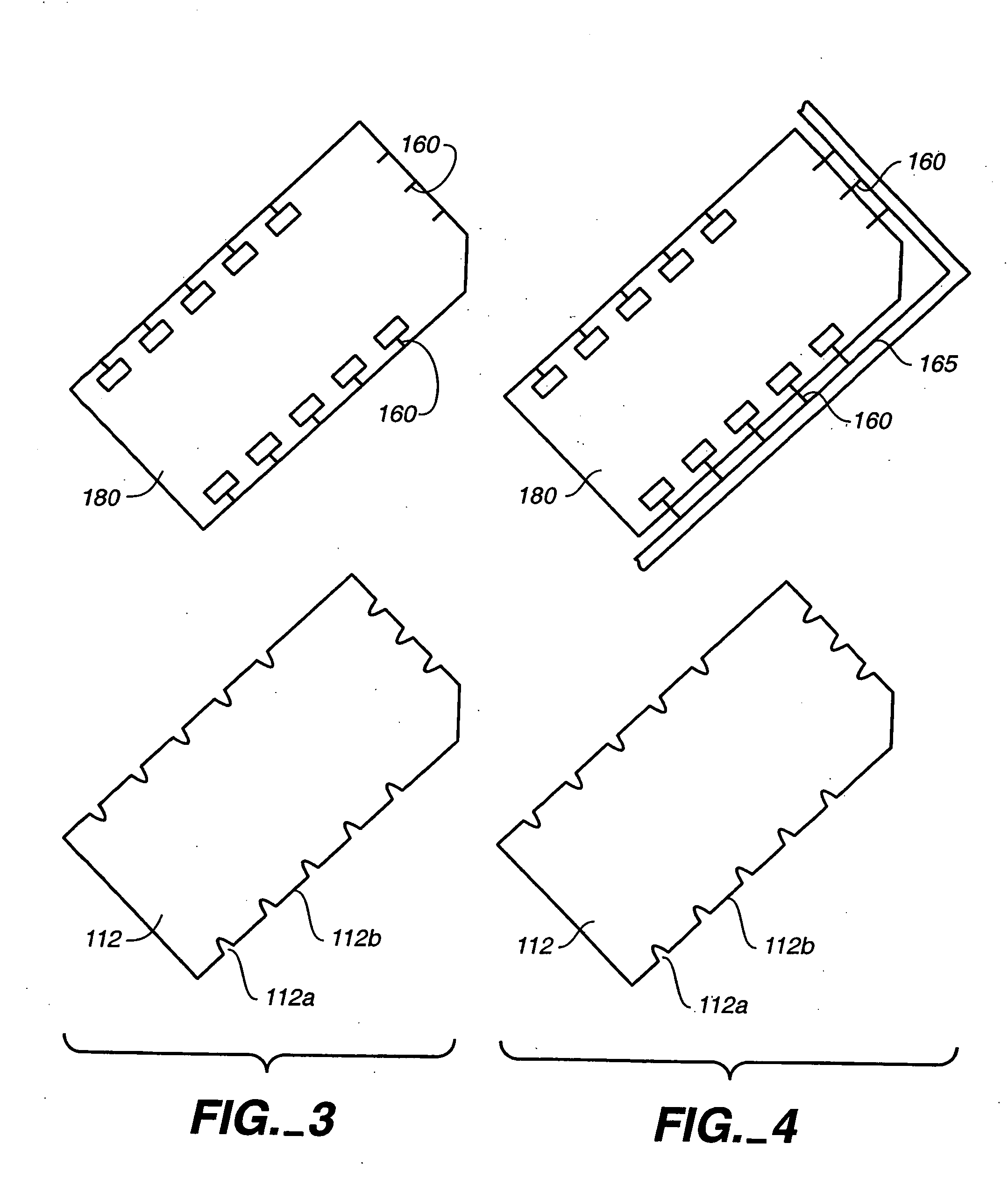
[0020]FIG. 1 shows the rear side of a memory card exemplifying the present invention. The memory card 100 comprises a circuit board 110 having an exposed rear side with terminals 140 and a covered front side (not shown). The covered side comprises at least one integrated circuit including flash memory, circuit traces, and passive components, which are not shown. Cover 120 covers over the front side and edges of the circuit board, such that the rear side of the circuit board is exposed to form substantially all of the rear side of the memory card. A narrow gap 130 at the junction between the edges of circuit board 110 and cover 120 exists. An electrostatic discharge 150 is shown entering the narrow gap 130 at the junction between the edges of circuit board 110 and cover 120. U.S. Pat. No. 6,040,622 to Wallace, entitled “Semiconductor Package Using Terminals Formed on a Conductive Layer of a Circuit Board” describes in detail the construction of a memory package in detail and is hereb...


PUM


Abstract

A card manufacturing technique and the resulting card are provided. The card has a ground and / or power layer extending to the edges of a circuit board for electrostatic discharge protection but also has gaps at the edge of the ground and / or power layer to avoid short circuiting with conductive segments of another layer deformed when the card is trimmed during manufacture.

Description

CROSS REFERENCE TO RELATED APPLICATIONS [0001] The present application is related to U.S. application Ser. No. 09 / 096,140 issued as U.S. Pat. No. 6,040,622 which is hereby incorporated by reference in its entirety.FIELD OF THE INVENTION [0002] The invention relates generally to circuit boards, a method of making a memory card integrating a circuit board, and the resulting memory card. BACKGROUND OF THE INVENTION [0003] This invention relates generally to circuit boards, and more specifically to circuit boards of memory cards utilized in portable devices to store data. Although the invention has application to a wide variety of circuit boards, it is described herein to be implemented in a memory card, specifically a portable memory card having flash electrically-erasable and programmable read-only memory (flash EEPROM). [0004] In recent years, devices such as digital cameras, digital audio players, and personal digital assistants have become popular. These devices require a large amo...

Claims


Application Information

Patent Timeline
Patent Type & Authority Applications(United States)
IPC IPC(8): H05K1/00H05K1/02H05K1/11G06K19/077H05K3/00H05K3/24H05K3/46
CPCG06K19/077H05K2203/175G06K19/07735H05K1/0256H05K1/0259H05K1/0268H05K1/0298H05K1/117H05K3/0052H05K3/242H05K2201/0919H05K2201/093H05K2201/09309H05K2201/0969G06K19/07732H01L2224/48091H01L2224/48227H01L2924/00014H05K1/11
Inventor WALLACE, ROBERT F.
Owner SANDISK TECH LLC
Why Eureka
Try Eureka