Silicide formation for a semiconductor device

a technology of semiconductor devices and silicides, applied in the field of semiconductor device silicide formation, can solve the problems of unacceptable sheet resistance of metal silicide layer on the gate, undesirably high sheet resistance,

Inactive Publication Date: 2005-04-28
FREESCALE SEMICON INC
View PDF16 Cites 18 Cited by
  • Summary
  • Abstract
  • Description
  • Claims
  • Application Information

AI Technical Summary

Problems solved by technology

However, a metal silicide formed on a gate may exhibit an undesirably high sheet resistance, especially for a device with a small linewidth.
For cobalt silicides, an undesirably high sheet resistance may be related to the unavailability of a sufficient number of nuclei on which the low resistivity CoSi2 phase nucleates.
This may lead to a non-uniform, discontinuous CoSi2 film with several voids, leading to unacceptable sheet resistance for the silicide layer on the gate.

Method used


Image

  • Silicide formation for a semiconductor device
  • Silicide formation for a semiconductor device
  • Silicide formation for a semiconductor device

Examples


Embodiment Construction

[0013] The following sets forth a detailed description of a mode for carrying out the invention. The description is intended to be illustrative of the invention and should not be taken to be limiting.

[0014] It has been discovered that implanting a gate with xenon ions prior to the formation of the gate silicide may reduce the sheet resistance of the gate silicide, thereby improving device characteristics and yield.

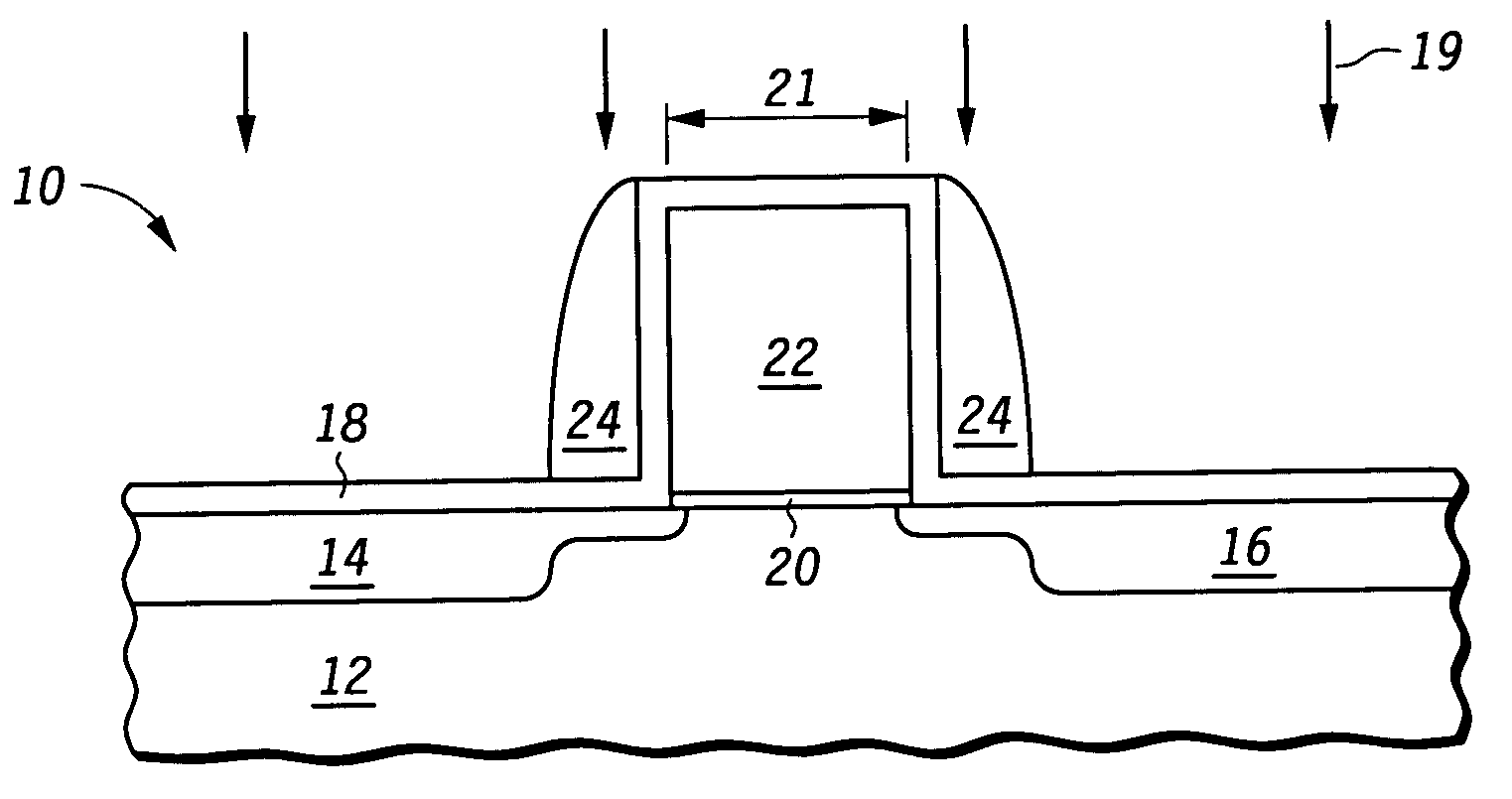
[0015]FIG. 1 is a partial cut away side view of a semiconductor wafer according to the present invention. Wafer 10 includes a semiconductor substrate 12 with a gate 22 formed there over. Source / drain regions 14 and 16 are located in substrate 12. In one embodiment, source / drain regions 14 and 16 have been formed by the ion implantation of a dopant (not shown) in those areas. In the embodiment shown, regions 14 and 16 are formed with two ion implants and a subsequent anneal with the first ion implant for implanting dopant for the source / drain extensions and a second ion i...


PUM

PropertyMeasurementUnit
sizesaaaaaaaaaa
sizesaaaaaaaaaa
sizesaaaaaaaaaa

Abstract

A polysilicon line (22), used e.g. as a gate, has a portion (30) amorphized by implanting (19) particles having a relatively large atomic mass. The amorphized portion is used to form a metal silicide (38) having a desirably low sheet resistance. Exemplary metals are cobalt and nickel that can provide the thin lines of below 50 nanometers. An exemplary particle for implanting that has sufficient atomic mass is xenon. The dose and the energy of the implant (19) are potentially different based on the linewidth (21) of the polysilicon line (22).

Description

BACKGROUND OF THE INVENTION [0001] 1. Field of the Invention [0002] This invention relates in general to semiconductor processing and more specifically to the formation of silicides. [0003] 2. Description of the Related Art [0004] Semiconductor device fabrication may involve forming silicides on the source / drain regions and a gate of a semiconductor device. However, a metal silicide formed on a gate may exhibit an undesirably high sheet resistance, especially for a device with a small linewidth. [0005] For cobalt silicides, an undesirably high sheet resistance may be related to the unavailability of a sufficient number of nuclei on which the low resistivity CoSi2 phase nucleates. This may lead to a non-uniform, discontinuous CoSi2 film with several voids, leading to unacceptable sheet resistance for the silicide layer on the gate. [0006] What is needed is an improved gate silicide.BRIEF DESCRIPTION OF THE DRAWINGS [0007] The present invention may be better understood, and its numero...

Claims


Application Information

Patent Timeline
Patent Type & Authority Applications(United States)
IPC IPC(8): H01L21/265H01L21/3205H01L21/336H01L21/425H01L21/4763H01L29/78
CPCH01L21/2652H01L29/665H01L29/7833H01L29/6659H01L29/6656H01L21/28518
Inventor JAWARANI, DHARMESH
Owner FREESCALE SEMICON INC
Why Eureka
Try Eureka