

Baths, methods, and tools for superconformal deposition of conductive materials other than copper
- Summary
- Abstract
- Description
- Claims
- Application Information
AI Technical Summary
Benefits of technology
Problems solved by technology
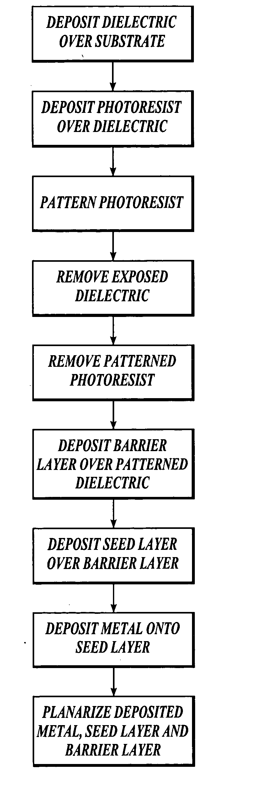
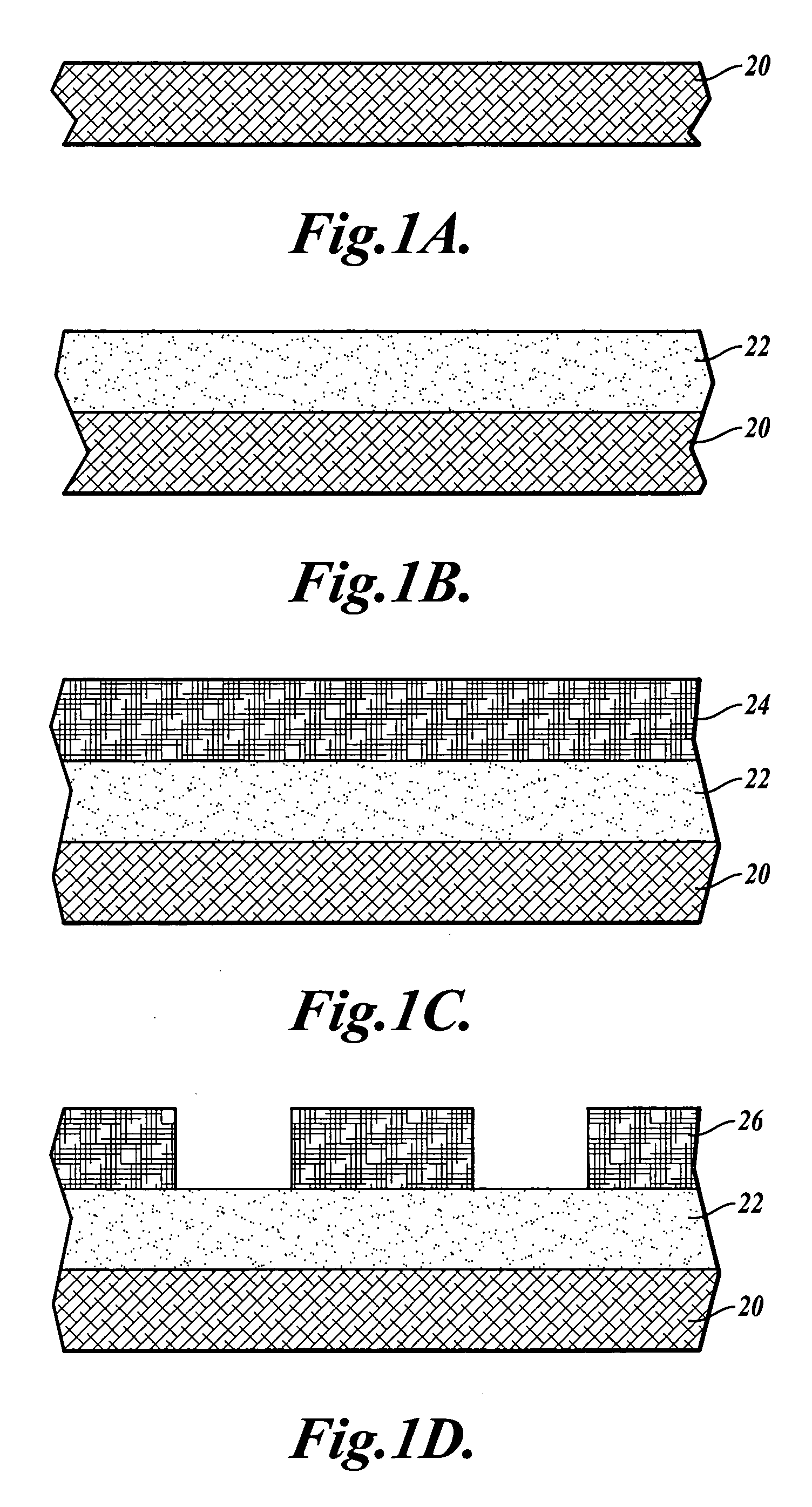
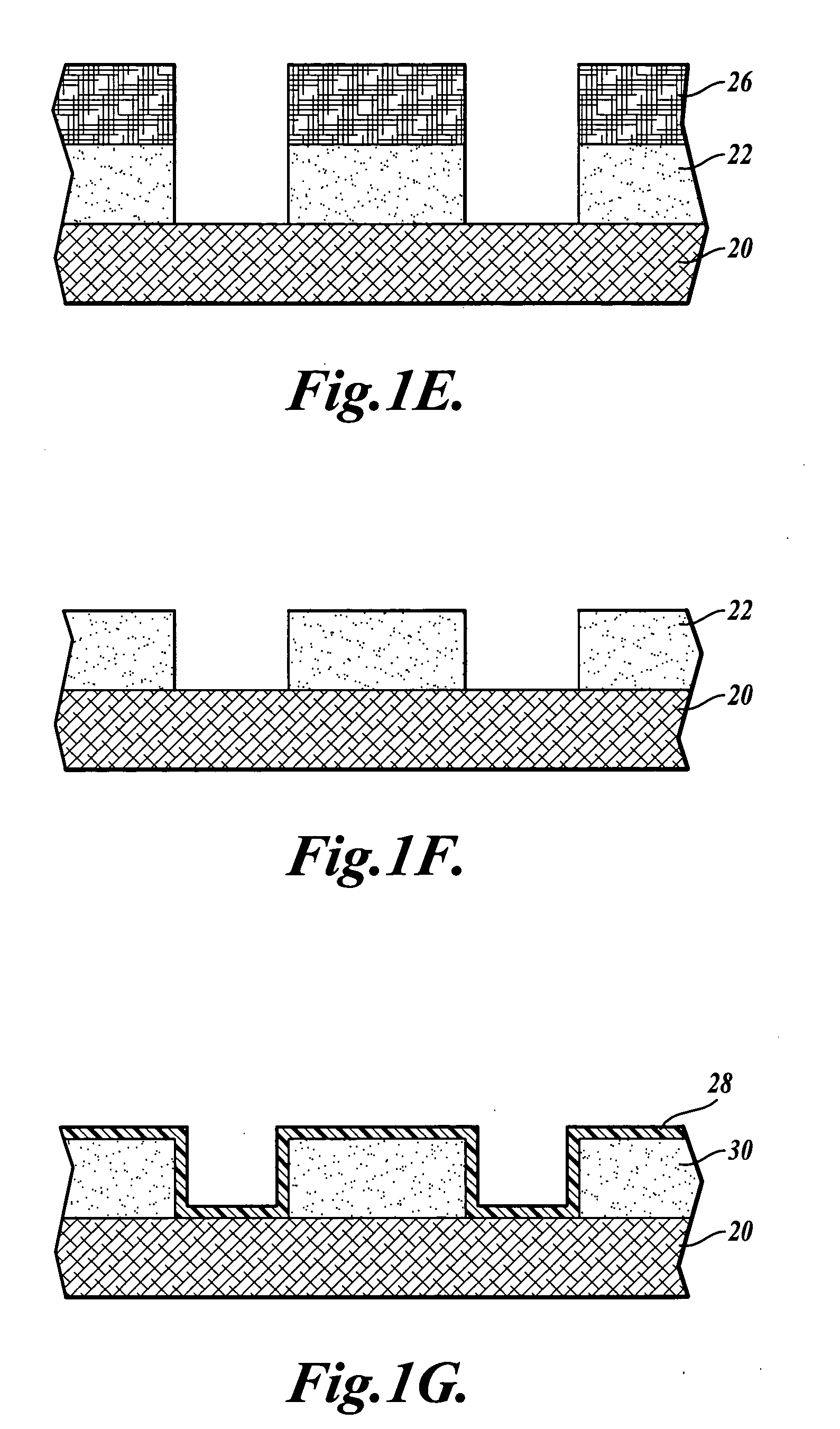
Method used
Image

Examples
example
Superconformal Electrolytic Deposition of Gold into Patterned Features
[0053] In this example, a silicon wafer including patterned features having a feature depth of 3.8 μm and an aspect ratio of 4:1 was processed to deposit gold into the patterned features superconformally. The patterned features included a titanium-based barrier layer 500 Å thick and a gold seed layer 500 Å thick. The titanium-based barrier layer and gold seed layer were deposited by sputtering. The wafer was contacted with the electroplating bath in an Equinox® brand single wafer plating tool available from Semitool, Inc. of Kalispell, Mont. The plating tool included an inert platinum anode. The plating was carried out at 50° C. The chemical flow rate was 3.5 gpm and the wafer was rotated at 40 rpm. The electroplating power was pulsed with 2 ms on and 8 ms off. The peak current density was 8 mA / cm2 and an average current density was 1.6 mA / cm2. This resulted in a plating rate of about 0.1 μm per minute.
[0054] The...
PUM
| Property | Measurement | Unit |
|---|---|---|
| Substance count | aaaaa | aaaaa |
| Electrical conductor | aaaaa | aaaaa |
| Deposition rate | aaaaa | aaaaa |
Abstract
Description
Claims
Application Information