Helical resonator type plasma processing apparatus

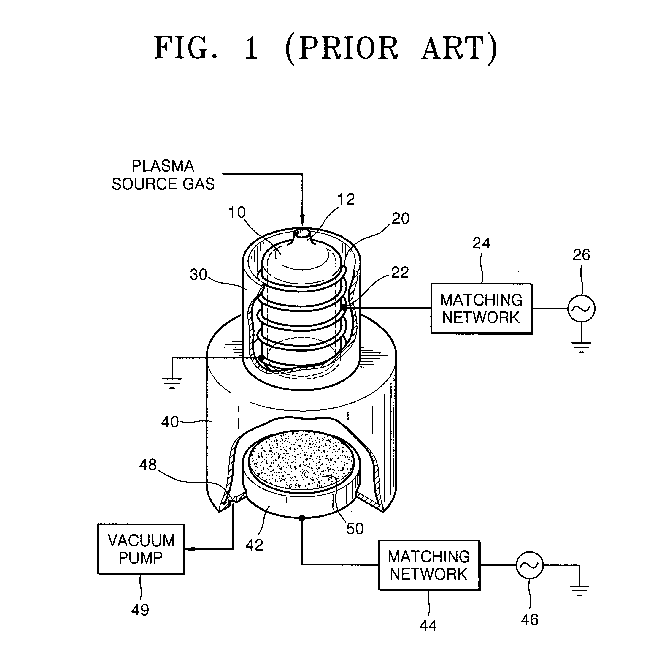
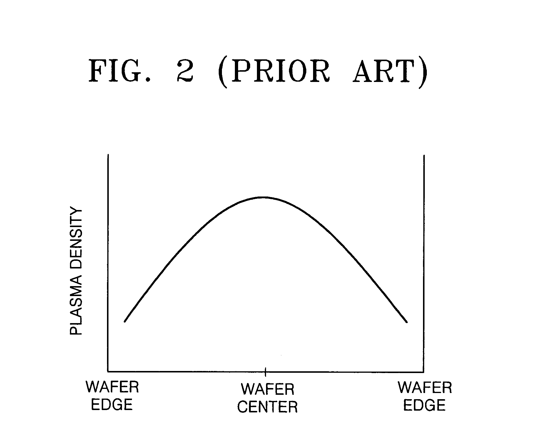
a plasma processing and helical resonator technology, applied in the field of plasma processing apparatus, can solve the problems of severer problems, the conventional helical resonator plasma processing apparatus has a difficulty in obtaining a uniform plasma density along the radial direction of the wafer, so as to achieve the effect of improving the density uniformity of plasma and easy control of plasma potential

Inactive Publication Date: 2005-05-05
SAMSUNG ELECTRONICS CO LTD
View PDF36 Cites 38 Cited by
  • Summary
  • Abstract
  • Description
  • Claims
  • Application Information

AI Technical Summary

Benefits of technology

[0032] The use of a plasma processing apparatus according to the present invention provides an improvement in density uniformity of plasma close to a wafer along the radial direction of the wafer, and an easy way to control a plasma potential in a process chamber.

Problems solved by technology

In spite of such structural advantage, the helical resonator plasma sources are not widely applied to semiconductor processes for etching or deposition because of difficulties in securing plasma density uniformity in radial directions of a wafer in a process chamber.
That is, the conventional helical resonator plasma processing apparatus has a difficulty in obtaining a uniform plasma density along the radial direction of the wafer 50.
Particularly, this problem becomes severer when the wafer50 has a large diameter.
These problems can significantly reduce the quality of semiconductor devices as well as the process yield.
However, a conventional helical resonator plasma processing apparatus has a drawback in adequately controlling the plasma potential for a particular process and process conditions.

Method used


Image

  • Helical resonator type plasma processing apparatus
  • Helical resonator type plasma processing apparatus
  • Helical resonator type plasma processing apparatus

Examples


Embodiment Construction

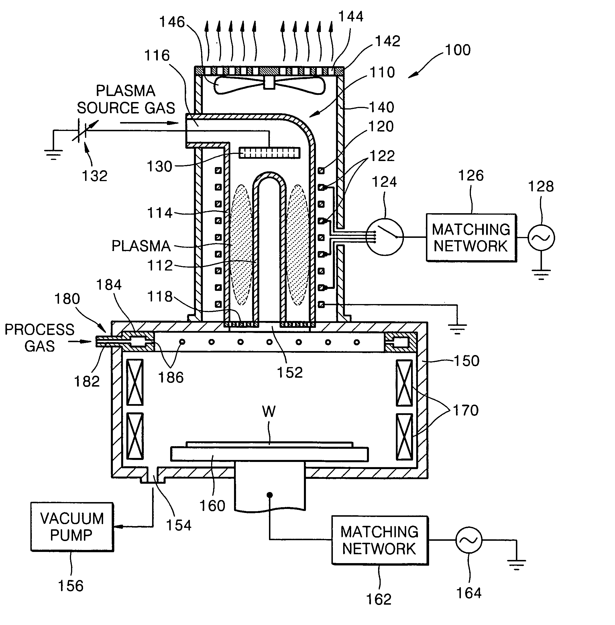
[0043] Hereinafter, the present invention will be described more fully with reference to the accompanying drawings in which preferred embodiments of the invention are shown by way of example. Like reference numerals refer to like elements throughout the drawings.

[0044]FIG. 3 is a vertical cross-sectional view of a helical resonator plasma processing apparatus according to a preferred embodiment of the present invention. FIG. 4 is a partially broken away perspective view of a dielectric tube, a control electrode, a helix coil, and the plasma distributor depicted in FIG. 3.

[0045] Referring to FIGS. 3 and 4, a helical resonator plasma processing apparatus according to the present invention is a sort of a semiconductor manufacturing apparatus for performing a fine processing such as etching a surface of a substrate or depositing a predetermined material layer on a substrate by using plasma produced by a helical resonator 100. The substrate which is loaded in a process chamber 150 can ...


PUM


Abstract

Provided is helical resonator plasma processing apparatus. The plasma processing apparatus comprises a process chamber having a substrate holder for supporting a substrate, a dielectric tube disposed on the process chamber to communicate with the process chamber, a helix coil wounded around the dielectric tube, and an RF power source to supply RF power to the helix coil. The dielectric tube has a double tube shape and comprises an inner tube and an outer tube, and a plasma source gas inlet port to supply plasma source gas into a space between the inner tube and the outer tube is disposed in the outer tube. A control electrode to control plasma potential is disposed in the dielectric tube. This plasma processing apparatus provides a uniform plasma density distribution along a radial direction of a wafer, and easy control of the plasma potential in the process chamber.

Description

BACKGROUND OF THE INVENTION [0001] This application claims the priority of Korean Patent Application No. 2003-77762 filed on Nov. 4, 2003, in the Korean Intellectual Property Office, the disclosure of which is incorporated herein in its entirety by reference. [0002] 1. Field of the Invention [0003] The present invention relates to a plasma processing apparatus, and more particularly, to a helical resonator type plasma processing apparatus using a helix coil. [0004] 2. Description of the Related Art [0005] Presently, plasma sources are widely used for processing fine semiconductor devices or flat display panels in the semiconductor industry. That is, plasma sources are becoming indispensable tools for etching thin films or deposition of predetermined thin material films on a surface of a wafer for manufacturing semiconductor devices or on a substrate for manufacturing a flat panel display such as an LCD. Accordingly, the development of an apparatus for processing plasma sources is be...

Claims


Application Information

Patent Timeline
Patent Type & Authority Applications(United States)
IPC IPC(8): H05H1/46H01J7/24H01J37/32H01L21/00H01L21/205H01L21/3065H05H1/00
CPCH01J37/321H01J37/32697H01J37/3211H01L21/00
Inventor KIM, DAE-ILMA, DONG-JOONKIM, GOOK-YOONCHOI, SUNG-KYU
Owner SAMSUNG ELECTRONICS CO LTD
Why Eureka
Try Eureka