Video signal processing system including analog to digital converter and related method for calibrating analog to digital converter
- Summary
- Abstract
- Description
- Claims
- Application Information
AI Technical Summary
Benefits of technology
Problems solved by technology
Method used
Image
Examples
first embodiment
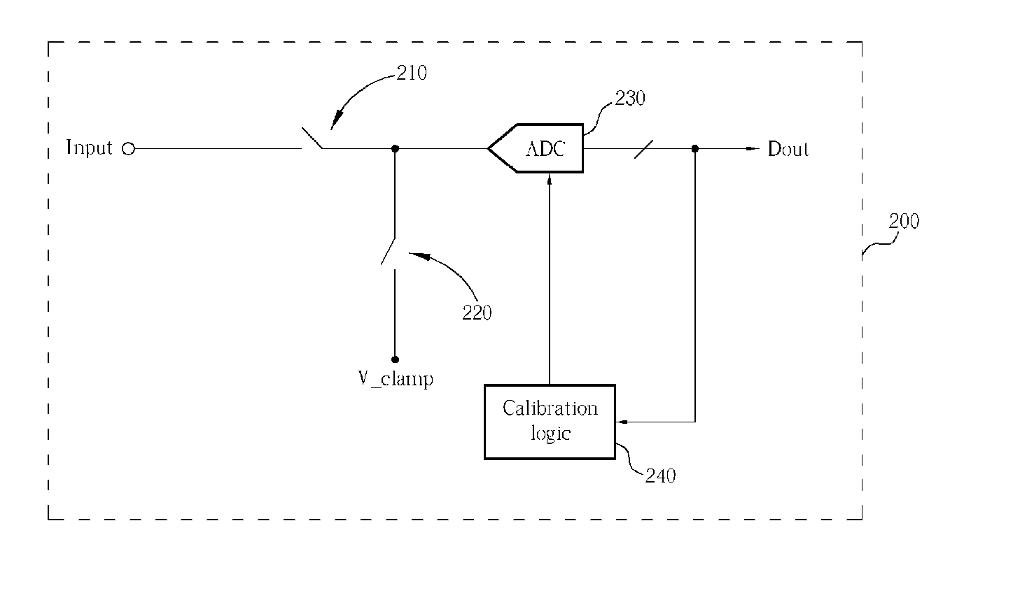
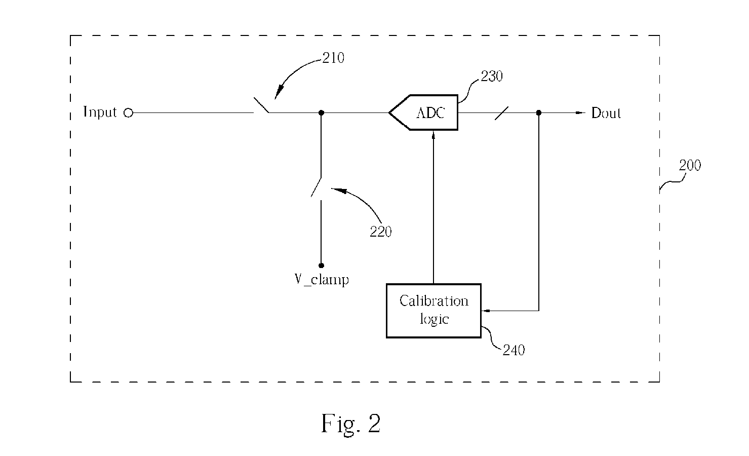
[0027] Please refer to FIG. 2. FIG. 2 is a block diagram of the present invention video signal processing system 200. In the present invention video signal processing system 200, one end of input switch 210 is coupled to ADC 230, and another end of input switch 210 is for receiving input video signals; one end of offset switch 220 is coupled to the ADC as well, and another end of offset switch 220 is for receiving a clamp reference voltage V_clamp, which is corresponding to a clamp level of video images to be processed; and calibration logic 240 is coupled to ADC 230 for adjusting an offset of ADC 230 according to output digits Dout of ADC 230. When input video signals have no content during a horizontal line period, since the video signal processing system only displays images of the lowest gray level stably, the present invention video signal processing system 200 can disconnect ADC 230 from video signals to be input, and display images of the lowest gray level automatically. Ther...
second embodiment
[0028] The present invention provides gain calibration of the ADC as well. Please refer to FIG. 3. FIG. 3 is a block diagram of the present invention video signal processing system 300. In the present invention video signal processing system 300, there is an input switch 310 playing the same role as the input switch 210 in the video signal processing system 200. There are two reference switches 321 and 322 for calibrating gain of ADC 330 in the present invention video signal processing system 300. The first reference switch 321 has a first end coupled to the input of ADC 330, and a second end for receiving a first reference voltage V_ref1. The second reference switch 322 has a first end coupled to the input of ADC 330 as well, and a second end for receiving a second reference voltage V_ref2. The first reference voltage V_ref1 and the second reference voltage V_rer2 are two predetermined values between a lowest voltage level and a highest voltage level of video images to be input to ...
third embodiment
[0029] Besides distortions in the internal circuit of the ADC, dc levels of video signals may drift in the system before entering the ADC. The variation of dc levels will destroy the conversion of ADC. Therefore, a calibration of dc levels of input video signals is highly preferred for improving performance of an ADC. The claimed invention introduces a video signal processing system and related method for serving to dc-shift input video signals to a predetermined level that matches the input range of the ADC. Please refer to FIG. 4. FIG. 4 is a block diagram of the present invention video signal processing system 400. The present invention video signal processing system 400 comprises a capacitor 405, a clamp switch 425, and an ADC 430. For adjusting dc-levels of input video signals, the clamp switch 425 is switched on to connect ADC 430 with a clamp reference voltage V_clamp, which is corresponding to the predetermined dc-level of video signals, when video signals are in black level...
PUM
 Abstract
Description
Claims
Application Information


