Memory card and semiconductor device

Inactive Publication Date: 2005-05-05
RENESAS ELECTRONICS CORP
View PDF12 Cites 21 Cited by
  • Summary
  • Abstract
  • Description
  • Claims
  • Application Information

AI Technical Summary

Benefits of technology

[0041] A memory card without any inconvenience caused by connecting a non-antenna to an antenna connecting pin can be implemented when the memory card is inserted into a card host for the memory card that does not correspond to a noncontact interface.
[0042] A memory card without any inconvenience caused by connecting an antenna to a pin that is independent of the antenna can be implemented when the memory card that does not correspond to a noncontact interface is inserted into a card host for the noncontact interface.

Problems solved by technology

One type of inconvenience is caused by connecting a non-antenna terminal of a card host to an antenna connecting pin of the memory card when the antenna connecting pin is enlarged to the memory card or an existing pin also serves as the antenna connecting pin, and the memory card that corresponds to the noncontact interface is inserted into a card host for an existing memory card.
The other type of inconvenience is caused by connecting an antenna terminal of the card host to a pin of the memory card unrelated to the antenna when an existing memory card is inserted into the card host for the noncontact interface.

Method used


Image

  • Memory card and semiconductor device
  • Memory card and semiconductor device
  • Memory card and semiconductor device

Examples


Embodiment Construction

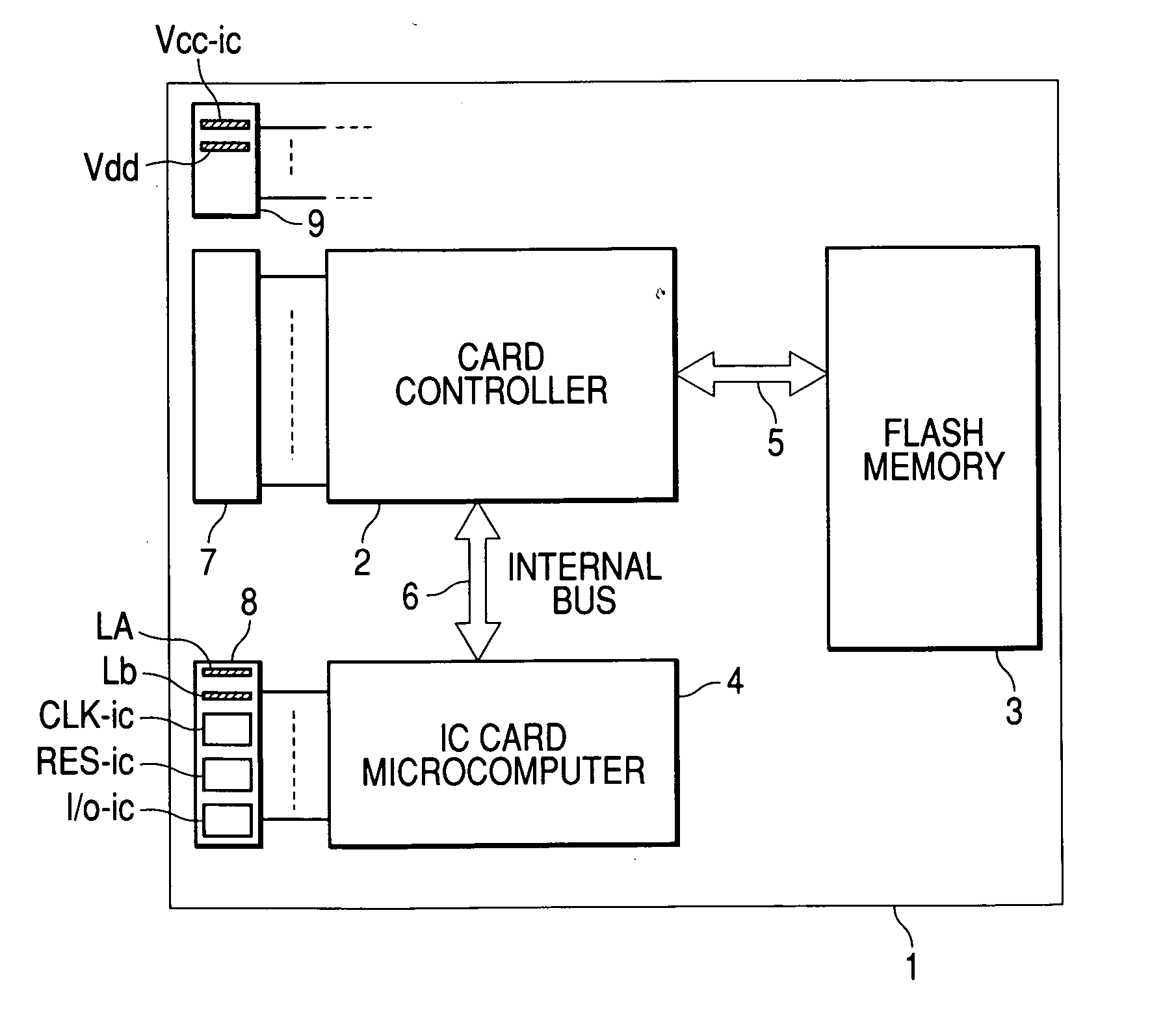
[0072]FIG. 1 shows a block diagram of a memory card conforming to the MultiMedia Card Standards that is an example of a semiconductor device according to the present invention. A memory card 1 shown in the same block diagram provides multifunctions, such as an information storage function and a security function accompanying cryptographic / decoding processing and authentication processing. The security function is utilized for settlement of accounts using a credit card or charging in transport facilities, for example.

[0073] The memory card 1 mounts a card controller 2, an electrically rewritable nonvolatile memory unit such as a flash memory 3 connected to the card controller 2 through an internal bus 5, and an IC (integrated circuit) card microcomputer (also referred to as an IC card microcomputer) 4 in a wiring substrate on which a plurality of external pins are formed. Although limited in particular, the card controller 2, the flash memory 3, and the IC card microcomputer 4 have ...


PUM


Abstract

An antenna connection function for a noncontact interface is provided by suppressing a modification in a pin arrangement and a pin shape of a memory card that does not correspond to the noncontact interface. Two antenna connecting pins having the memory card are divided into two areas in which a size of one potential supply pin is the largest and used as a split pin arranged at intervals. Because a size of the two antenna connecting pins is at maximum as large as the size of the potential supply pin, the two antenna connecting pins are provided and the memory card that corresponds to the noncontact interface is obtained by devoting a pin area having the size of the one potential supply pin to the memory card that does not correspond to the noncontact interface. Accordingly, the pin area of the memory card that corresponds to the noncontact interface can be formed without departing from the pin area of the memory card that does not correspond to the noncontact interface.

Description

CROSS-REFERENCE TO RELATED APPLICATION [0001] The present application claims priority from Japanese application JP 2003-374237 filed on Nov. 4, 2003, the content of which is hereby incorporated by reference into this application. BACKGROUND OF THE INVENTION [0002] The present invention relates to noncontact interface technology in a card device or in a semiconductor device that is typical of a memory card, and antenna connection technology for a noncontact interface, and, for example, relates to an effective technology for applying to the noncontact interface of the memory card that mounts an IC card microcomputer together with a card controller and a nonvolatile memory. [0003] Patent Reference 1 describes technology by which an SIM (subscriber identity module) is mounted in a memory card conforming to MMC (MultiMedia Card: registered mark) Standards and security is enhanced so that multibanks or multifunctions can be implemented maintaining compatibility with the MultiMedia Card St...

Claims


Application Information

Patent Timeline
Patent Type & Authority Applications(United States)
IPC IPC(8): G06K19/00G06K19/077G11C7/00
CPCG06K19/005G06K19/07749G06K19/07732G06K19/077
Inventor NISHIZAWA, HIROTAKAHIGUCHI, AKIRAOSAWA, KENJIOSAKO, JUNICHIROWADA, TAMAKISUGIYAMA, MICHIAKI
Owner RENESAS ELECTRONICS CORP
Why Eureka
Try Eureka