System for search and analysis of systematic defects in integrated circuits

a systematic and integrated circuit technology, applied in image analysis, image enhancement, instruments, etc., can solve the problems of systematic defects relating to layout design flaws or processing design flaws, which will occur regularly, and yield characterization engineers face a difficult task in identifying the cause of such defects. , to achieve the effect of convenient searching

Inactive Publication Date: 2005-05-05
GLOBALFOUNDRIES INC
View PDF11 Cites 17 Cited by
  • Summary
  • Abstract
  • Description
  • Claims
  • Application Information

AI Technical Summary

Benefits of technology

[0007] Alternatively, the regular grid of windows is replaced by a randomly placed set of windows, in order to avoid any spatial phase correlations of windows to patterns and to control the amount of data processed and retained for the indexing and search process.
[0008] After performing the extracting and index processing, the invention performs the process of feature searching by first identifying a defect region window of the circuit layout and similarly merging basis patterns with shapes in the defect region window. This merging process can include transforming, rotating and mirroring the layout shapes in the defect region. The invention similarly transforms shapes in the defect region window into defect vectors by finding intersections between basis patterns and the shapes in the defect region to facilitate searching. Then, the invention can easily find feature vectors that are similar to the defect vector using, for example, representative feature vectors from the index of feature vectors. Then, the similarities and differences between the defect vectors and the other feature vectors can be analyzed.
[0009] Before the comparing process, the invention can perform adaptive sampling on the feature vectors to eliminate redundant feature vectors. After the comparing process, the invention stores the feature vectors and the index in a database, wherein the database is used for multiple different feature searching processes. The invention also maintains coordinate location information of the windows corresponding to each feature vectors within the circuit design.

Problems solved by technology

Systematic defects in a semiconductor process are those defects which are not a result of particles interfering with exposure or other process steps during manufacturing.
Instead, systematic defects relate to layout design flaws or processing design flaws and will occur regularly at the same location within a finished product.
Yield characterization engineers face a difficult task in identifying the cause of such defects.
Particularly, in modern processes requiring resolution enhancement, chemo-mechanical polishing and other complex steps, the root cause often involves the interaction of a particular local pattern with the shapes in its context.
The same pattern which results in a deterministic fail (or is not robust to process variations) in a particular part may not fail in other locations on the same design, or on a different design.

Method used


Image

  • System for search and analysis of systematic defects in integrated circuits
  • System for search and analysis of systematic defects in integrated circuits
  • System for search and analysis of systematic defects in integrated circuits

Examples


Embodiment Construction

[0018] The present invention and the various features and advantageous details thereof are explained more fully with reference to the nonlimiting embodiments that are illustrated in the accompanying drawings and detailed in the following description. It should be noted that the features illustrated in the drawings are not necessarily drawn to scale. Descriptions of well-known components and processing techniques are omitted so as to not unnecessarily obscure the present invention in detail.

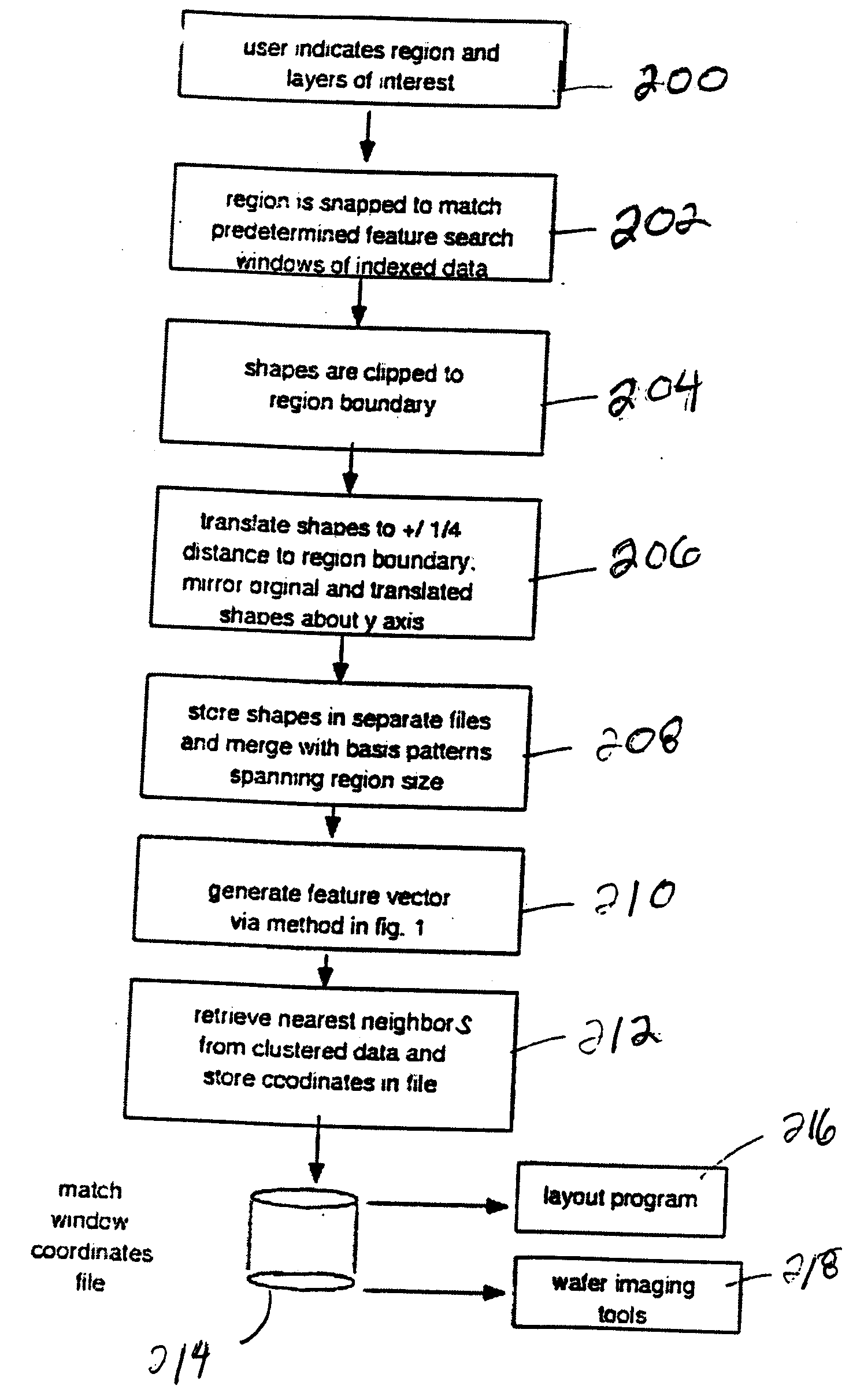
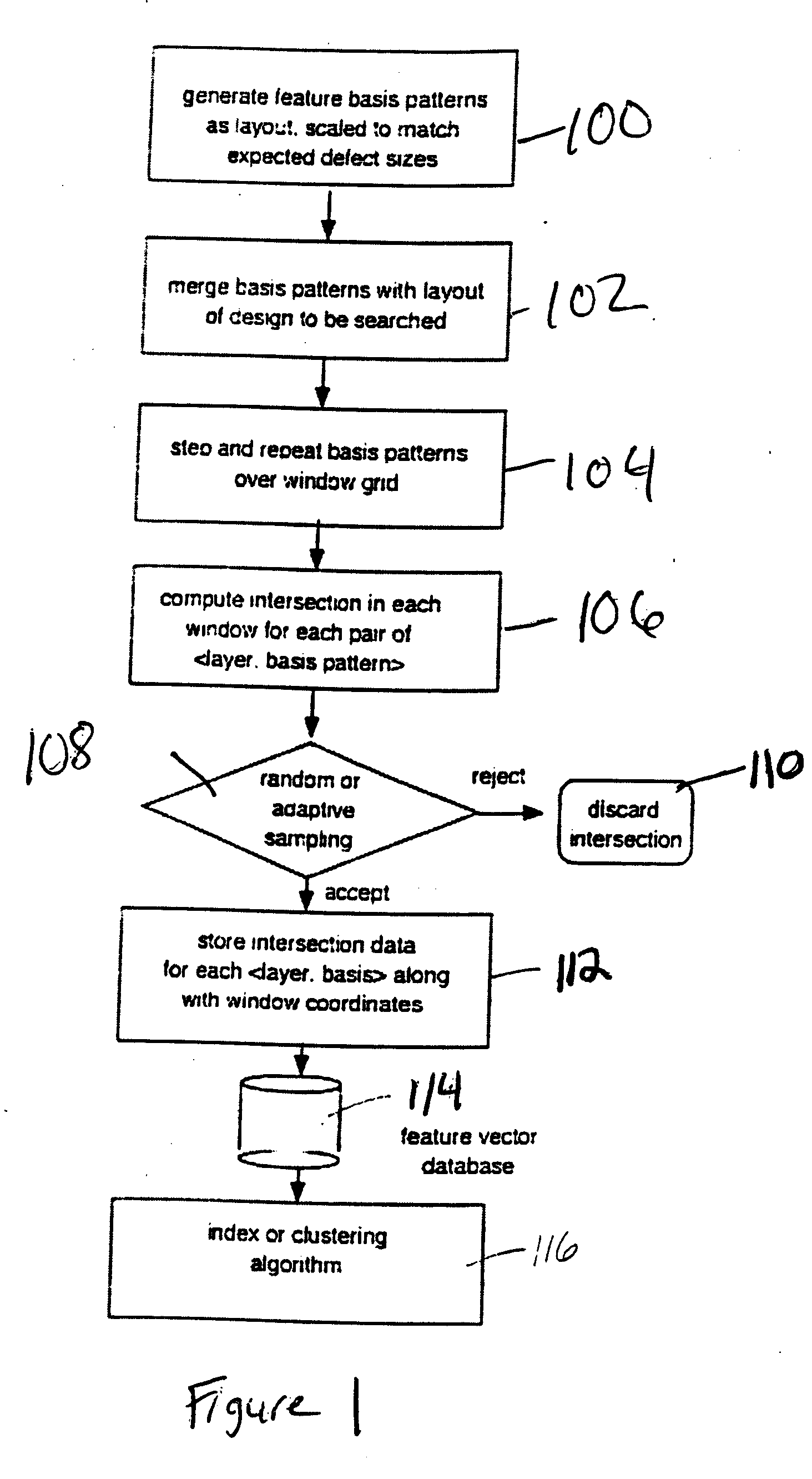
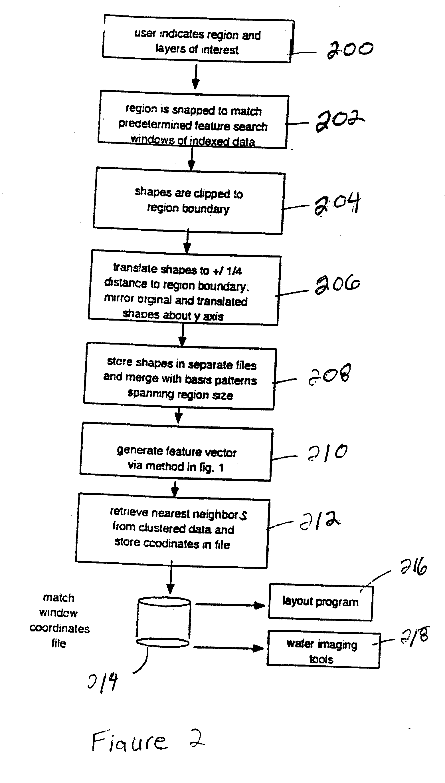
[0019] As mentioned above, yield characterization engineers face a difficult task in identifying the cause of systematic defects. The problem faced by the engineers encountering a systematic failure is formulated as a search task. With the invention, feature vectors of defect shapes and nearby shape context (defect vectors) are compared to a previously established database of feature vectors for the circuit to see whether systematic failures occur in areas where similar patterns to the defect sha...


PUM


Abstract

Disclosed is a method of locating systematic defects in integrated circuits. The invention first performs a preliminary extracting and index processing of the circuit design and then performs feature searching. When performing the preliminary extracting and index processing the invention establishes a window grid for the circuit design and merges basis patterns with shapes in the circuit design within each window of the window grid. The invention transforms shapes in a each window into feature vectors by finding intersections between the basis patterns and the shapes in the windows. Then, the invention clusters the feature vectors to produce an index of feature vectors. After performing the extracting and index processing, the invention performs the process of feature searching by first identifying a defect region window of the circuit layout and similarly merging basis patterns with shapes in the defect region window. This merging process can include rotating and mirroring the shapes in the defect region. The invention similarly transforms shapes in the defect region window into defect vectors by finding intersections between basis patterns and the shapes in the defect region. Then, the invention can easily find feature vectors that are similar to the defect vector using, for example, representative feature vectors from the index of feature vectors. Then, the similarities and differences between the defect vectors and the feature vectors can be analyzed.

Description

BACKGROUND OF INVENTION [0001] 1. Field of the Invention [0002] The present invention generally relates to a system for identifying and analyzing systematic defects in integrated circuits. [0003] 2. Description of the Related Art [0004] Systematic defects in a semiconductor process are those defects which are not a result of particles interfering with exposure or other process steps during manufacturing. Instead, systematic defects relate to layout design flaws or processing design flaws and will occur regularly at the same location within a finished product. Yield characterization engineers face a difficult task in identifying the cause of such defects. Particularly, in modern processes requiring resolution enhancement, chemo-mechanical polishing and other complex steps, the root cause often involves the interaction of a particular local pattern with the shapes in its context. The same pattern which results in a deterministic fail (or is not robust to process variations) in a parti...

Claims


Application Information

Patent Timeline
Patent Type & Authority Applications(United States)
IPC IPC(8): G06K9/00G06T7/00
CPCG06T2207/30148G06T7/001
Inventor BERGMAN REUTER, BETTE L.DEMARIS, DAVID L.LAVIN, MARK A.LEIPOLD, WILLIAM C.MAYNARD, DANIEL N.MUKHERJEE, MAHARAJ
Owner GLOBALFOUNDRIES INC
Why Eureka
Try Eureka