High-density packaging of integrated circuits

a technology of integrated circuits and high density, applied in the direction of color television, semiconductor/solid-state device details, television systems, etc., can solve the problems of increasing the transistor count, producing complex and sophisticated integrated circuit architectures, and reducing the size of transistors, etc., to meet the demand for more transistors

Inactive Publication Date: 2005-05-05
SAPIR ITZHAK
View PDF1 Cites 26 Cited by
  • Summary
  • Abstract
  • Description
  • Claims
  • Application Information

AI Technical Summary

Benefits of technology

[0013] The present invention solves these and other problems by providing a technique for folding a relatively large substrate to produce an integrated circuit having a much smaller form-factor than the original (unfolded) circuit. The smaller form-

Problems solved by technology

The demand for faster, cheaper and more versatile circuits has given the electronics industry the incentive to increase the transistor count and produce complex and sophisticated integrated circuit architectures.
As transistors became faster, interconnection delays started to become significant.
Unfortunately, t

Method used


Image

  • High-density packaging of integrated circuits
  • High-density packaging of integrated circuits
  • High-density packaging of integrated circuits

Examples


Embodiment Construction

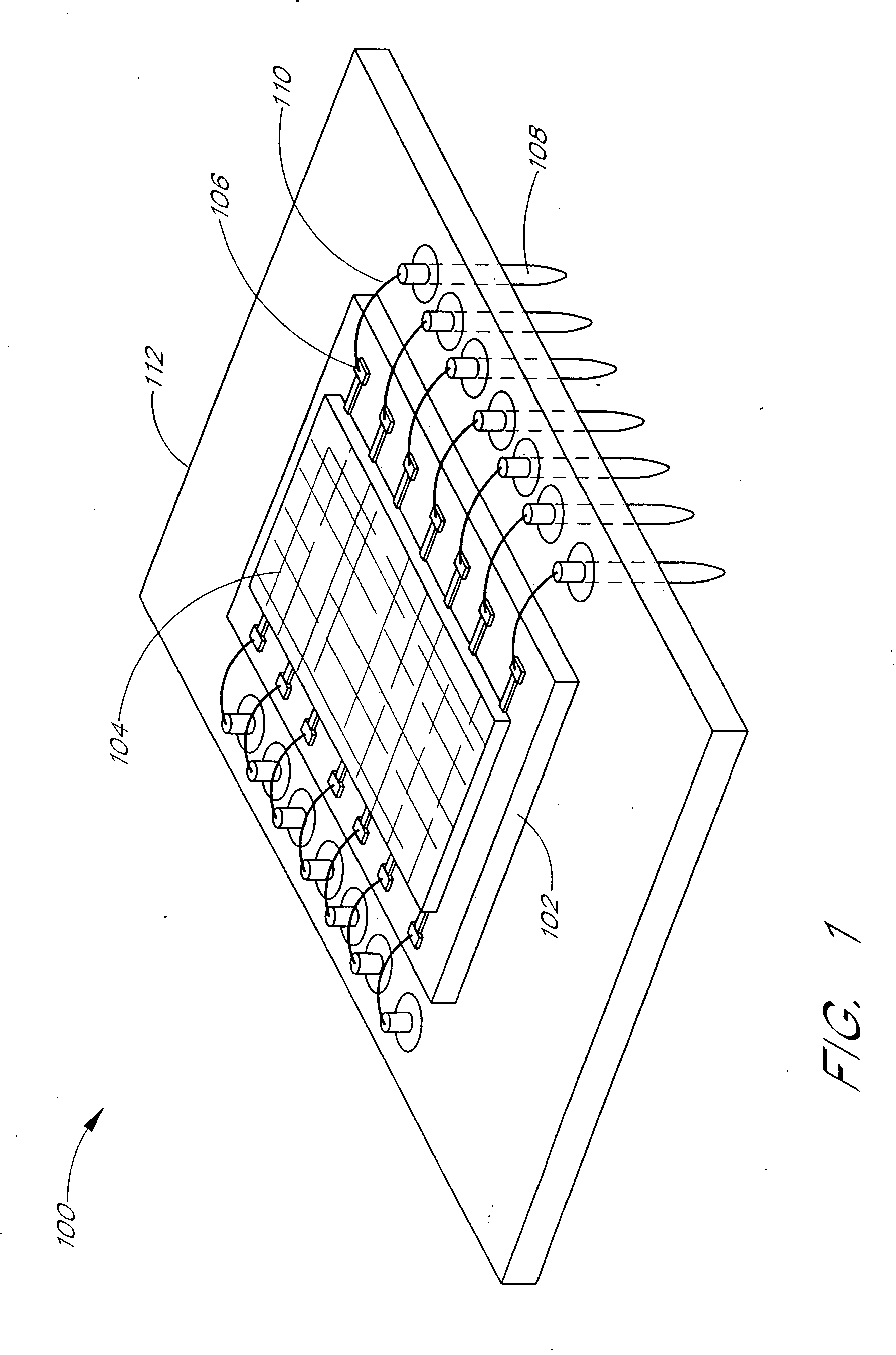
[0033]FIG. 1 shows a typical packaged integrated circuit 100. The integrated circuit 100 includes a silicon substrate 102 having an active region 104. The active region 104 includes various electronic components (e.g., transistors, resistors, capacitors, etc.) formed by doping and lithography processes (such as, for example, the processes described in connection with FIGS. 2-8). The substrate 102 is attached to a carrier 112. The carrier 112 has one or more contacts, such as a contact pin 108. A wire 110 is attached to the pin 108 and to a contact pad 106 deposited on the substrate 102. One or more conducting traces provide electrical connection between the contact pad 106 and the components in the active region 104. For convenience, and not by way of limitation, the substrate in the following disclosure is described as being made of silicon. One of ordinary skill in the art will recognize, however, that the integrated circuit substrate can be made of other elements, alloys, or comp...


PUM


Abstract

An integrated circuit constructed on a folded integrated circuit is described. The folded integrated circuit has a much smaller form-factor than the original (unfolded) circuit and is thus more suitable for use in miniature devices, such as, for example, electronic camera, electronic-film cartridge, cellular telephone, handheld computer, handheld digital music device, portable devices, handheld devices, and the like. In one embodiment, the integrated circuit is folded by thinning an area of the substrate such that the thinned area of the substrate becomes flexible. Conducting traces on the upper surface of the substrate connect an active region on one side of the thinned area to an active region on the other side of the thinned area. The substrate is folded at the thinned area to thereby reduce the size of the substrate. In one embodiment, a heat-sink is inserted between the folds to carry heat away from the substrate.

Description

RELATED APPLICATIONS [0001] The present application is a continuation of application Ser. No. 09 / 616,432, filed Jul. 14, 2000, which claims priority under 35 U.S.C. 119(e) from U.S. Provisional Application No. 60 / 144,433, filed on Jul. 17, 1999, titled “E-FILM TECHNOLOGY,” both of which are hereby incorporated by reference.BACKGROUND OF THE INVENTION [0002] 1. Field of the Invention [0003] The invention relates to techniques for construction of densely packed integrated circuits using folded silicon substrates. [0004] 2. Description of the Related Art [0005] An integrated circuit is a device consisting of many interconnected transistors and other components fabricated on a (typically) silicon wafer. The silicon wafer is known as the “substrate”. Different areas of the substrate are “doped” with other elements to make either “P-type” or “N-type” regions, and conducting tracks are placed in layers over the surface. The die is then typically connected into a package using gold wires th...

Claims


Application Information

Patent Timeline
IPC IPC(8): H01L21/822H01L27/04H04N5/225
CPCH01L21/822H04N5/225H04N1/2116H01L27/04H04N23/00
Inventor SAPIR, ITZHAK
Owner SAPIR ITZHAK
Why Eureka
Try Eureka